
Global Service
Three-dimensional integrated circuits (3DICs) have emerged as a promising solution to meet the increasing demands for high performance and compactness in modern applications. By stacking individual ICs/wafers together as a single package, 3DIC technology offers several advantages over traditional two-dimensional (2D) integrated circuits.
The TAIHOYA ATMS Dynamic Culture System is a cell mechanobiology platform that closely aligns with the FDA’s policy direction.
PLP 自動化解決方案:產品背景與設計概念
粒徑分析的樣品前處理|雷射粒徑分析量測困難樣品完整指南
In the era of Advanced Packaging (e.g., CoWoS, Chiplet), heterogeneous integration introduces complex material interfaces. Consequently, thermal stress and warpage have made Delamination a primary yield killer.
During laser or X-ray inspection, fully packaged HBM shows fewer electrical anomalies, while exposed advanced DRAM requires much stricter control of energy and exposure. Does this mean HBM DRAM is inherently more resistant?
The evolution of semiconductor technologies into sub-10 nm nodes and 3D architectures like high-bandwidth memory (HBM), even small static potentials can result in critical device failures. The effectiveness of DC ionization compared to AC systems, especially for protecting advanced packaging structures such as micro-bumps and TSVs. As semiconductor processes scale down and packaging grows more complex, controlling ESD during wet cleaning and drying becomes essential.
Test wafers play an indispensable role in the semiconductor industry, fulfilling various functions that are vital for manufacturing, failure analysis and quality assurance of semiconductor devices. Test wafers are of paramount importance in ensuring the reliability and efficiency of semiconductor devices and technologies.
Handling ultrathin wafers and reducing wafer thickness without damaging the pre-process has been a challenging task for semiconductor industries. Temporary bonding and debonding (TBDB) technology was developed to address this.
As Moore’s Law approaches its physical limits, the semiconductor industry has shifted its focus from transistor scaling alone to innovation in advanced packaging. Packaging is no longer merely a means of chip protection; it has become a primary driver of system-level performance gains.
In semiconductor manufacturing, dicing or singulation is a critical process that separates individual dies from a processed wafer. Whether performed mechanically or with lasers, this step introduces significant physical stress on the wafer, which may lead to chipping or cracking of the silicon (Si) substrate.
Failure modes in advanced packaging are concentrating around invisible defects. These are not issues you can identify with surface checks. In many cases, only X-ray inspection can reveal internal bonding integrity without damaging the sample.
Micro bumps are critical miniature solder interconnects used in advanced packaging technologies. Their size is typically below 40 μm, and can even shrink to 10–20 μm, which is significantly smaller than traditional BGA (diameter > 500 μm) or flip chip bumps (diameter ~80–120 μm). They are used to enable high-density interconnections between die-to-die or die-to-interposer.
Handling and processing thin wafers mounted on a frame post-debonding, along with the subsequent cleaning process, presents formidable challenges in advanced semiconductor packaging technologies. Conventional cleaning methods carry the risk of damaging thinned wafers.
In modern semiconductor process, removing the photoresist is a critical step. After the lithography process, the exposed photoresist must be removed from the wafer surface to reveal the patterned areas for further processing.
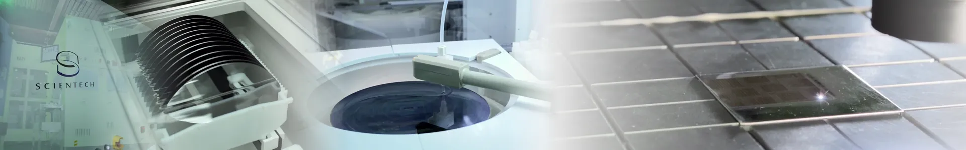
Scientech’s wet process equipment has been successfully implemented in the fabrication of the recent chipset 3DIC, CoWoS and advanced packaging process.
As advanced packaging moves toward high I/O density and heterogeneous integration, icro bumps have become a key technology for high-density chip-to-chip interconnects. They offer smaller sizes and higher I/O density compared to traditional solder balls, and are widely used in 2.5D, 3D IC, Chiplet, and high-frequency/high-speed component packaging.
When most people think about “medical device risk,” their first instinct is: Will it fail? Will it break? In real-world use, however, the most critical concern for patients is infection.
The semiconductor industry is undergoing a profound transformation as devices demand higher performance, smaller form factors, and lower power consumption. Traditional packaging approaches are no longer sufficient to meet the requirements of AI accelerators, high-performance computing (HPC), 5G communication, autonomous vehicles, and consumer electronics, all of which rely heavily on advanced packaging technologies to enable higher bandwidth, greater interconnect density, and improved thermal management.
Wafer warpage is a critical challenge in advanced semiconductor processes, particularly with thin wafers, heterogeneous integration. Warpage can lead to misalignment, transfer failures, and significant yield loss. To tackle these challenges, Scientech together with AMC has developed an integrated solution tailored to modern manufacturing demands.
In the era of Advanced Packaging (e.g., CoWoS, Chiplet), heterogeneous integration introduces complex material interfaces. Consequently, thermal stress and warpage have made Delamination a primary yield killer.


