As Moore’s Law approaches its physical limits, the focus of the semiconductor industry has shifted from simple “transistor scaling” to “innovation in packaging technologies.” Packaging is no longer merely a means of protecting chips, it has become a key battlefield for performance enhancement.
Stage 1: Traditional Packaging
Traditional packaging primarily refers to fixing a single die onto a substrate, connecting it via wire bonding or leads, and encapsulating it in a plastic shell for protection. Its main functions are to provide power, heat dissipation, and physical protection.
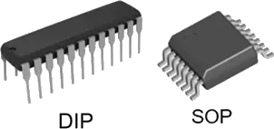
- Early Stage: DIP (Dual in-line Package) & SOP (Small Outline Package)
DIP (Dual In-line Package) features two parallel rows of metal pins that can be inserted into a socket.
SOP (Small Outline Package) is a miniaturized version of DIP, which later evolved into variants such as SOJ, TSOP, VSOP, SSOP, TSSOP, SOT, and SOIC.
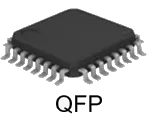
- Mid-Stage: QFP (Quad Flat Package)
This stage saw the introduction of the “Lead Frame”. QFP is a surface-mount package with L-shaped pins extending from all four sides.
- Late Stage: BGA (Ball Grid Array)
BGA replaces pins with tiny solder balls arranged in a grid pattern. This significantly increases the I/O count and allows the chip to connect directly to the Printed Circuit Board (PCB). The shorter connections (solder balls) reduce parasitic inductance and capacitance, leading to superior signal performance. Heat is efficiently conducted from the chip to the PCB, enhancing system stability. 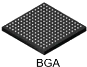
Stage 2: WLP and SiP (Wafer-Level & System-Level Packaging)
This stage marks the transition from single-chip packaging to multi-functional integration, such as wafer-level packaging (WLP) and system-in-package (SiP), aiming to reduce size and increase signal transmission speeds. Wafer-level packaging (WLP) and system-in-package (SiP) are two key packaging technologies in the modern semiconductor industry for achieving thin, light, and high-performance electronic products.
- WLP (Wafer-Level Package):
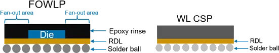
This process involves packaging and testing the entire silicon wafer before dicing, which effectively minimizes the package size. The packaged size is roughly the same as the die itself, making it the smallest packaging method currently available. WLP eliminates the need for wire bonding and lead frames. It uses RDL (Redistribution Layer) technology to rearrange contacts into a matrix, connecting the wafer to the substrate via bumping. Because wire bonding or lead frames are omitted, the signal transmission path is extremely short, which is beneficial for high-frequency computing and further reduces package size. Wafer-level packaging (WLP) can be divided into fan-in WLP and fan-out WLP based on input/output (I/O) connections
Fan-In WLP: Routing is confined within the die size, suitable for chips with low I/O counts.
Fan-Out WLP: To accommodate higher I/O counts, RDL is used to extend the routing beyond the die's footprint.
- SiP (System-in-Package):
This technology integrates multiple chips with different functions (e.g., processors, memory, sensors) and passive components (e.g., resistors, capacitors) into a single package. It enables full system functionality within one unit, achieving miniaturization, high performance, low power consumption, and shorter development cycles. 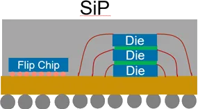
Stage 3: Advanced Packaging
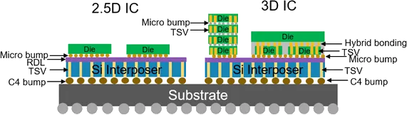
Advanced Packaging is the core technology for breaking through the physical limits of Moore's Law and continuously improving chip performance. Unlike traditional packaging, which only provides mechanical protection and basic conductivity, it focuses on Heterogeneous Integration, integrating chips with different processes and functions (such as CPU, GPU, and HBM) with extremely tight spacing to achieve low power consumption, high bandwidth, and small footprints. Currently, the mainstream technologies are 2.5D packaging and 3D packaging. 2.5D packaging, such as CoWoS, places system-on-a-chip (SoC), memory and other chips on a silicon interposer. They are linked via RDL and micro bumps for smooth electronic signal transmission, then connects them to the underlying substrate through silicon interposer and C4 bumps. 3D packaging, chips are vertically stacked and connected via micro bumps or hybrid Bonding. These stacks connect to the interposer through TSV (Through-Silicon Via) and micro bumps. Hybrid bonding, with its bumpless design, offers unprecedented interconnect density.