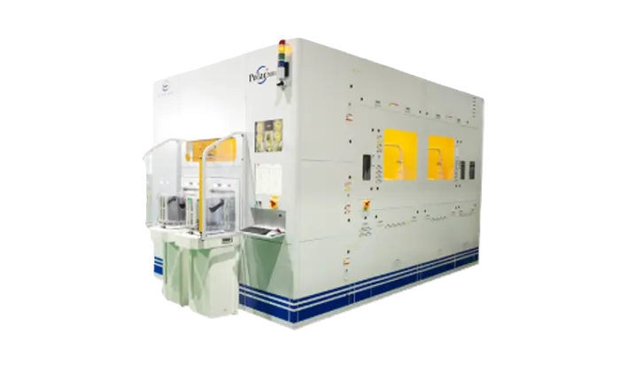
Glass Release Layer Coating-Pyxis RL Series
Scientech, in collaboration with global leader 3M, has developed the Pyxis series Glass Releasing Layer Coating Equipment which provides solutions for glass releasing layer coating in wafer thinning, BGBM (Backside Grinding & Backside Metallization), and advanced semiconductor packaging processes.
Related Products
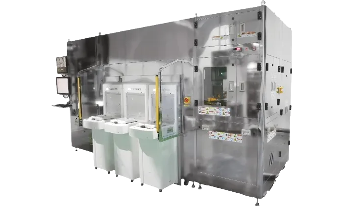
Glass Release Layer Coating
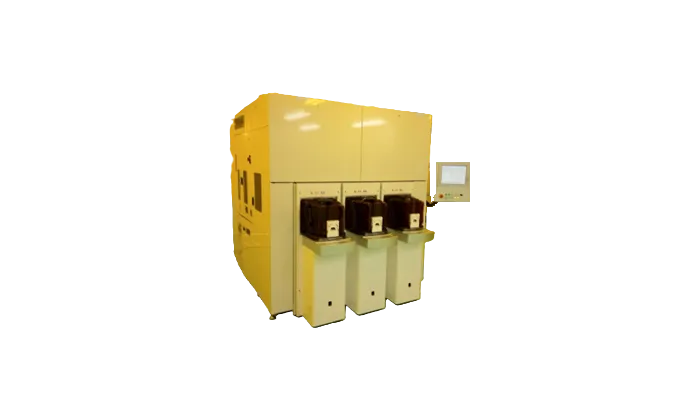
Temporary Bonding
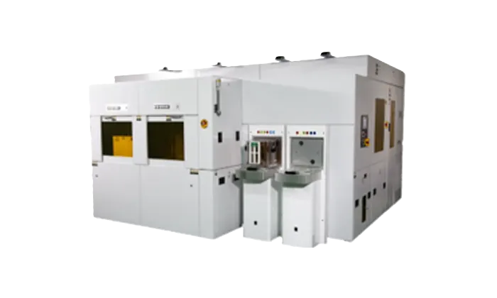
Debonding
Debonding Cleaning