ATMS: Your Key to Leading the FDA's New Era of Non-Animal Drug Evaluation.
The TAIHOYA ATMS Dynamic Culture System is a cell mechanobiology platform that closely aligns with the FDA’s policy direction.
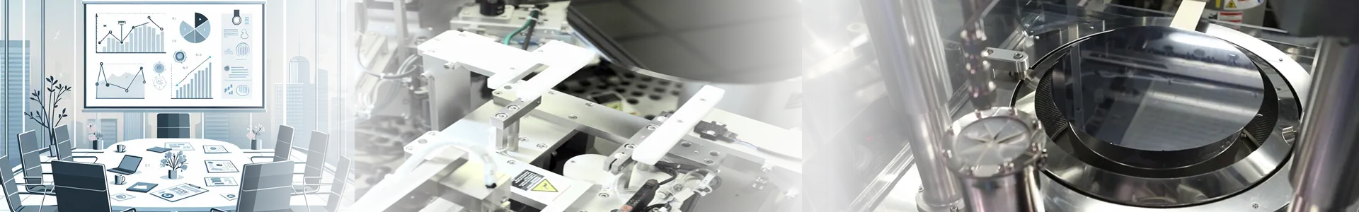
Wafer warpage is a critical challenge in advanced semiconductor processes, particularly with thin wafers, heterogeneous integration. Warpage can lead to misalignment, transfer failures, and significant yield loss. To tackle these challenges, Scientech together with AMC has developed an integrated solution tailored to modern manufacturing demands.
The evolution of semiconductor technologies into sub-10 nm nodes and 3D architectures like high-bandwidth memory (HBM), even small static potentials can result in critical device failures. The effectiveness of DC ionization compared to AC systems, especially for protecting advanced packaging structures such as micro-bumps and TSVs. As semiconductor processes scale down and packaging grows more complex, controlling ESD during wet cleaning and drying becomes essential.
In semiconductor manufacturing, dicing or singulation is a critical process that separates individual dies from a processed wafer. Whether performed mechanically or with lasers, this step introduces significant physical stress on the wafer, which may lead to chipping or cracking of the silicon (Si) substrate.
Handling and processing thin wafers mounted on a frame post-debonding, along with the subsequent cleaning process, presents formidable challenges in advanced semiconductor packaging technologies. Conventional cleaning methods carry the risk of damaging thinned wafers.


