
Skip to header Skip to main navigation Skip to main content

Main navigation

  • Home
      • Profile
      • Organization
      • ESG
      • Inclusive Workplace
      • Certificates
      • Responsible Purchase
      • Public Relations
      • Global Presence
      • Business Conduct
      • Inquiry
      • Product List
      • Camera Lens
      • Chemical Biotechnology
      • Diffusion
      • Thin Film
      • Etching
      • Lithography
      • Metrology, Inspection & Others
      • Repair & Calibration
      • Wet Bench
      • Single Wafer
      • Advanced Baking
      • Release Layer Coating
      • Batch Panel-level Wet Process
      • Single Panel-level Wet Process
      • Glass Release Layer Coating
      • Temporary Bonding
      • Debonding & Cleaning
      • Debonding
      • 12" Wafer Reclaim
      • Message from the Chairman
      • ESG Committee
      • Stakeholders
      • Materiality Issues
      • Integrity and Pragmatism
      • Supportive Workplace
      • ECO friendly
      • Social Contribution
      • GHG Emissions
      • Photo Gallery
      • ESG Report
      • Welfare
      • Job Search
      • Learning and Development
      • Fundamentals
      • Monthly Revenue
      • Annual Reports
      • Board of Directors
      • Committees
      • Internal Audit
      • Risk Management
      • Major Internal Policies
      • Status Report
      • Shareholders' Meeting
      • Investor Conference
      • Stock Quotes
      • TWSE MOPS
      • Contacts
      • Latest News
      • Event List
      • Newsletter
  • English
  • 繁體中文
辛耘公司 SCIENTECH
SCIENTECH CORPORATION
We Make It SIMPLE

SCIL

Breadcrumb

  • Home
  • SCIL

SCIL's technology began to take shape at Philips Research in 2001, and in 2015, Philips Research and Philips Intellectual Property & Standards decided to move the technology from "laboratory research and development" to "industrial mass production." SCIL Nanoimprint Solutions was thus born. Its first step was to design and build a fully automated machine specifically for imprinting nanopatterns onto substrates. The SCIL team gradually grew into a cross-disciplinary professional team. In 2023, SCIL Nanoimprint Solutions received funding from institutions across Europe and officially spin-out from Philips, embarking on a new path of development.
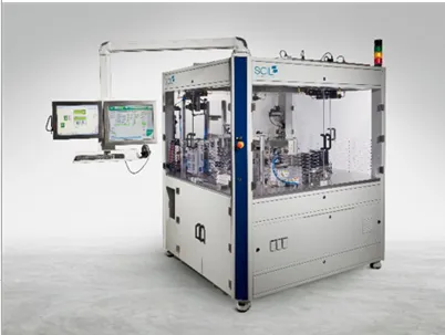
AutoSCIL

Use the arrow keys to navigate between tabs

AutoSCIL is an all-in-one system designed for laboratory research and development, process development, proof-of-concept (PoC) and pilot runs. Hardware and space design: It adopts a highly integrated enclosed chassis design, integrating all core functions such as wafer handling, pre-alignment, photoresist spin coating, capillary imprinting, and baking into a single machine space. Its small footprint makes it ideal for deployment in space-constrained R&D cleanrooms.

Features

  • Up to 700 imprints can be achieved with a single stamp, significantly reducing production costs compared to conventional technologies.
  • The proprietary resist features rapid curing without the need for additional UV exposure. Its high etching selectivity also eliminates the need for traditional hard masks (hard mask - SiO2, Si3N4, etc.), saving both process steps and costs for the production line.  
  • Direct face-to-face flat-press imprinting delivers significantly higher alignment accuracy compared to the rolling method.
  • All-in-one system with spin coating
  • Wafer cassette rack position
  • 100, 150 and 200mm wafers
  • Double side alignment  
  • Optical I/O
  • Silicon Photonics, CPO
  • CW laser/EML laser
  • Laser Polarizers
  • Face Recognition Sensors
  • Metalens
  • Waveguides

FabSCIL

Use the arrow keys to navigate between tabs

Briefly

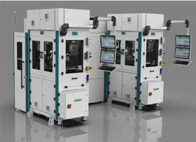
  • FabSCIL is a high-end lithography system designed for high-volume production.
  • Breaking away from the limitations of standalone systems, it adopts an advanced cluster design. The entire system consists of multiple independent process modules connected in series, including multiple independent spin-coating modules, curing/baking modules, and a central high-efficiency robotic arm. This architecture allows customers to "freely configure and expand" the system according to production line capacity bottlenecks to achieve maximum overall equipment efficiency (OEE).

Features

  • Up to 700 imprints can be achieved with a single stamp, significantly reducing production costs compared to conventional technologies.
  • The proprietary resist features rapid curing without the need for additional UV exposure. Its high etching selectivity also eliminates the need for traditional hard masks (hard mask - SiO2, Si3N4, etc.), saving both process steps and costs for the production line.  
  • Direct face-to-face flat-press imprinting delivers significantly higher alignment accuracy compared to the rolling method.

  • Cluster design, freely configurable
  • Spincoating, curing, etc
  • Wafer cassette loading station
  • 150, 200 and 300mm wafers
  • Double side alignment 
  • Optical I/O
  • Silicon Photonics, CPO
  • CW laser/EML laser
  • Laser Polarizers
  • Face Recognition Sensors
  • Metalens
  • Waveguides

Global Service

Location Detail

Social Media

Interactive Online

Contact Us

Leave Your Message

Affiliates

China | USA | Europe

Visiting Application

Visitor Portal

Vendor Management

Vendor Portal

About Us
Profile
Core Values
Contact Us
Product & Service
Representative
Own-Branding
Wafer Reclaim
ESG
Chairman's Words
Stakeholders
Reports
Careers
Development
Welfare
Job Search
Investors
Monthly Revenue
Annual Reports
Conference
Press Center
Latest News
Events
Newsletter

Copyright ©SCIENTECH. All trademarks and images are the property of their respective owners and protected by law.