
Skip to header Skip to main navigation Skip to main content

Main navigation

  • Home
      • Profile
      • Organization
      • ESG
      • Inclusive Workplace
      • Certificates
      • Responsible Purchase
      • Public Relations
      • Global Presence
      • Business Conduct
      • Inquiry
      • Product List
      • Camera Lens
      • Chemical Biotechnology
      • Diffusion
      • Thin Film
      • Etching
      • Lithography
      • Metrology, Inspection & Others
      • Repair & Calibration
      • Wet Bench
      • Single Wafer
      • Advanced Baking
      • Release Layer Coating
      • Batch Panel-level Wet Process
      • Single Panel-level Wet Process
      • Glass Release Layer Coating
      • Temporary Bonding
      • Debonding & Cleaning
      • Debonding
      • 12" Wafer Reclaim
      • Message from the Chairman
      • ESG Committee
      • Stakeholders
      • Materiality Issues
      • Integrity and Pragmatism
      • Supportive Workplace
      • ECO friendly
      • Social Contribution
      • GHG Emissions
      • Photo Gallery
      • ESG Report
      • Welfare
      • Job Search
      • Learning and Development
      • Fundamentals
      • Monthly Revenue
      • Annual Reports
      • Board of Directors
      • Committees
      • Internal Audit
      • Risk Management
      • Major Internal Policies
      • Status Report
      • Shareholders' Meeting
      • Investor Conference
      • Stock Quotes
      • TWSE MOPS
      • Contacts
      • Latest News
      • Event List
      • Newsletter
  • English
  • 繁體中文
辛耘公司 SCIENTECH
SCIENTECH CORPORATION
We Make It SIMPLE

UNISERS AG

Breadcrumb

  • Home
  • UNISERS AG

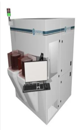
UNISERS, a cutting-edge semiconductor metrology and defect control startup headquartered in Zurich, Switzerland (founded in 2019 as an ETH Zurich spinoff), is dedicated to solving the most challenging nanoscale particle contamination problems in next-generation chip manufacturing. The company's flagship product, the UNISERS Explorer, is a revolutionary automated in-line 300mm wafer defect review system. Its greatest breakthrough lies in providing "molecular-level" chemical identification for extremely tiny defect particles, helping wafer fabs trace the sources of contamination at lightning speed and boost chip yields.
Sorter

Use the arrow keys to navigate between tabs

Briefly

1. (Molecular Particle Characterization):
2. (Revolutionary Sensitivity):
3. (Innovative Signal Enhancement)
4. (Yield & Cost Savings): 

Features

  • Molecular Particle CharacterizationUnlike traditional inspection equipment that can only "see" a defect, Explorer analyzes the molecular composition of particles. It precisely identifies whether the contaminant is a metal, organic material, silica, or another specific substance. This allows engineers to immediately target the exact processing tool or pipeline causing the pollution.
  • Revolutionary Nanoscale SensitivityUtilizing proprietary optical and physical technologies, the system captures and identifies extremely tiny nanoparticles down to 8 nanometers (nm) in size.
  • Innovative Signal EnhancementExplorer combines two proprietary technologies:Vacuum Plasma Coating Technology: It applies a temporary, specialized thin film to the wafer surface, making tiny impurities "glow" under optical microscopes to drastically boost visibility.Surface-Enhanced Raman Spectroscopy (SERS): It records the "molecular fingerprint" of individual nanoparticles, enabling high-speed, high-precision contamination identification.
  • Yield and Cost SavingsThrough real-time, in-line review, wafer fabs catch tool anomalies early in the process before contamination spreads. This prevents entire batches of wafers from being scrapped, thereby optimizing production yields and reducing carbon emissions.

  • Tool IntegrationAutomation: Automated in-line system.Modules: Equipped with standard EFEM (Equipment Front End Module) and FOUP load ports.
  • Factory Connection: Enables seamless, direct integration with the wafer fab's Automated Material Handling System (AMHS).
  • Product SpecificationsApplicable Wafer Size: Standard 300 mm (12-inch) wafers.
  • Process Compatibility: Supports advanced logic processes (3nm and below) and high-end memory processes.

Global Service

Location Detail

Social Media

Interactive Online

Contact Us

Leave Your Message

Affiliates

China | USA | Europe

Visiting Application

Visitor Portal

Vendor Management

Vendor Portal

About Us
Profile
Core Values
Contact Us
Product & Service
Representative
Own-Branding
Wafer Reclaim
ESG
Chairman's Words
Stakeholders
Reports
Careers
Development
Welfare
Job Search
Investors
Monthly Revenue
Annual Reports
Conference
Press Center
Latest News
Events
Newsletter

Copyright ©SCIENTECH. All trademarks and images are the property of their respective owners and protected by law.