Skip to header Skip to main navigation Skip to main content

Main navigation

  • Home
      • Profile
      • Organization
      • ESG
      • Inclusive Workplace
      • Certificates
      • Responsible Purchase
      • Public Relations
      • Global Presence
      • Business Conduct
      • Inquiry
      • Product List
      • Camera Lens
      • Chemical Biotechnology
      • Diffusion
      • Thin Film
      • Etching
      • Lithography
      • Metrology, Inspection & Others
      • Repair & Calibration
      • Wet Bench
      • Single Wafer
      • Advanced Baking
      • Release Layer Coating
      • Batch Panel-level Wet Process
      • Single Panel-level Wet Process
      • Glass Release Layer Coating
      • Temporary Bonding
      • Debonding & Cleaning
      • Debonding
      • 12" Wafer Reclaim
      • Message from the Chairman
      • ESG Committee
      • Stakeholders
      • Materiality Issues
      • Integrity and Pragmatism
      • Supportive Workplace
      • ECO friendly
      • Social Contribution
      • GHG Emissions
      • Photo Gallery
      • ESG Report
      • Welfare
      • Job Search
      • Learning and Development
      • Fundamentals
      • Monthly Revenue
      • Annual Reports
      • Board of Directors
      • Committees
      • Internal Audit
      • Risk Management
      • Major Internal Policies
      • Status Report
      • Shareholders' Meeting
      • Investor Conference
      • Stock Quotes
      • TWSE MOPS
      • Contacts
      • Latest News
      • Event List
      • Newsletter
  • English
辛耘公司 SCIENTECH
SCIENTECH CORPORATION
We Make It SIMPLE

Quantum

Breadcrumb

  • Home
  • Clone of Camtek

QuantumDiamonds is a global leader in quantum sensing technology for semiconductor analysis, delivering advanced solutions for non-destructive, high-resolution 3D failure analysis. Leveraging the unique properties of nitrogen-vacancy (NV) centers in diamond, our systems enable direct visualization of electrical activity and current flow- capabilities that go far beyond conventional techniques.


Our technology empowers semiconductor manufacturers to identify, localize, and understand failure mechanisms faster and more accurately, reducing time-to-root-cause and accelerating yield improvement. By bridging cutting-edge quantum physics with real-world engineering challenges, QuantumDiamonds is redefining how the industry approaches failure analysis and paving the way for more reliable and efficient next-generation devices.
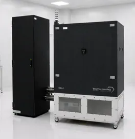
Use the arrow keys to navigate between tabs

The FRT MicroProf series is a high-precision metrology solution designed for the semiconductor industry, enabling comprehensive geometric measurements of wafers, including thickness, TTV (Total Thickness Variation), Bow, Warp, TIR (Total Indicated Runout), and LTV (Local Thickness Variation). Utilizing a white light source and a dual-probe configuration (top and bottom), the system performs non-contact measurements by positioning the wafer between the probes, allowing for efficient and accurate analysis in a single pass.

An optional infrared (IR) probe enhances measurement capabilities by enabling penetration of materials like silicon (Si) and gallium arsenide (GaAs), making it ideal for monitoring thickness changes during the backside thinning process. The system supports both manual and automated configurations to meet varying production needs.

  • Standard fixture supports samples from 2 to 12 inches
  • Measures thickness, TTV, Bow, and Warp on opaque and transparent materials
  • Optional IR probe for non-destructive layer thickness measurement on Si/GaAs
  • Ideal for incoming inspection, EPI process monitoring, and thinning process control
  • Available in manual (MicroProf 200/300) and automated (MicroProf 200/300 MHU) models
  • Integrated mapping function for multi-point measurement and wafer map generation
  • Built-in reference wafers for fast and accurate thickness calibration
  • Compound Semiconductors: GaAs, InP, SiC, GaN
  • Front-End Silicon Devices: Power devices, MEMS, RF MEMS
  • Back-End Silicon Devices: 8” and 12” packaging and bumping lines
  • Optical Communication: Quartz materials
  • 化合物半導體:GaAs,InP, SiC,GaN
  • 矽基元件前段:功率元件,MEMS,射頻MEMS
  • 矽基元件後段:8”和12”的封裝及bumping線
  • 光通訊:石英材料類

Global Service

Location Detail

Social Media

Interactive Online

Contact Us

Leave Your Message

Affiliates

China | USA | Europe

Visiting Application

Visitor Portal

Vendor Management

Vendor Portal

About Us
Profile
Core Values
Contact Us
Product & Service
Representative
Own-Branding
Wafer Reclaim
ESG
Chairman's Words
Stakeholders
Reports
Careers
Development
Welfare
Job Search
Investors
Monthly Revenue
Annual Reports
Conference
Press Center
Latest News
Events
Newsletter

Copyright ©SCIENTECH. All trademarks and images are the property of their respective owners and protected by law.