Skip to header

Main navigation

辛耘公司 SCIENTECH SCIENTECH
      • Profile
      • Core Value
      • Organization
      • ESG
      • Inclusive Workplace
      • Certificates
      • Public Relations
      • Global Presence
      • Product List
      • Camera Lens
      • Wet Bench
      • Single Wafer
      • Advanced Baking
      • Release Layer Coating
      • Batch Panel-level Wet Process
      • Single Panel-level Wet Process
      • Glass Release Layer Coating
      • Temporary Bonding
      • Debonding & Cleaning
      • Debonding
      • 12" Wafer Reclaim
      • Message from the Chairman
      • ESG Committee
      • Stakeholders
      • Materiality Issues
      • Integrity and Pragmatism
      • Supportive Workplace
      • ECO friendly
      • Social Contribution
      • GHG Emissions
      • Photo Gallery
      • ESG Report
      • Welfare
      • Job Search
      • Learning and Development
      • Fundamentals
      • Annual Reports
      • Monthly Revenue
      • Board of Directors
      • Committees
      • Internal Audit
      • Risk Management
      • Major Internal Policies
      • Status Report
      • Shareholders' Meeting
      • Investor Conference
      • Stock Quotes
      • TWSE MOPS
      • Contacts
      • Latest News
      • Event List
      • Newsletter
  • English
  • 繁體中文
SCIENTECH

MUETEC

Breadcrumb

  • Home
  • MUETEC

MueTec offers a comprehensive portfolio of Automated Optical Inspection (AOI) systems tailored for the wafer and photomask industries. Key applications include Critical Dimension (CD) and overlay metrology, defect inspection and review, as well as film thickness measurement. These advanced metrology and inspection solutions are engineered to help semiconductor fabs accelerate development and production ramp-up, maximize die yield, and enhance return on investment.
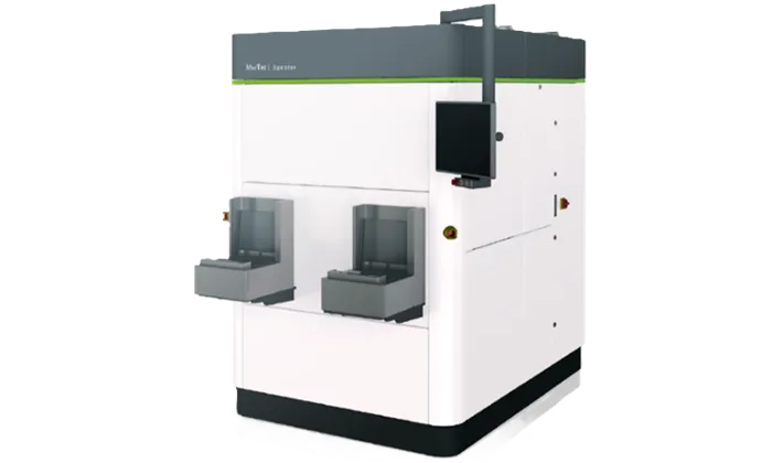
DaVinci 270UV

Use the arrow keys to navigate between tabs

MueTec has established a large global installed base of optical Critical Dimension (CD) mask metrology systems. These systems were previously marketed under the “LWM270UV” brand by Leica and KLA. The newest addition to this product line is the DaVinci 270UV—a fully enclosed, fully automated mask metrology system designed for precision and ease of use.

Key Features

  • Cost-effective solution for mask layers with feature sizes of 300 nm and larger
  • Supports both UV and visible light illumination
  • Operates in reflected and transmitted light modes
  • Equipped with high-quality optics
  • Available in flexible tool configurations
  • CD repeatability (3 sigma) over long term < 4 nm for etched layers
  • Mask Critical Dimension Metrology 

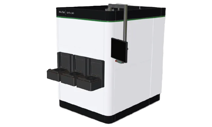
DaVinci 200 (CD, OVL, IR)

Use the arrow keys to navigate between tabs

MueTec’s infrared solutions are engineered to enhance manufacturing yield in MEMS production. These systems are available as fully automated solutions for 100 mm, 150 mm, 200 mm, and 300 mm MEMS wafers.

Key Features

  • Best-in-class IR image quality with wavelengths up to 1500 nm
  • Flexible wafer handling options including backside vacuum, flipping, and edge vacuum for MEMS-specific substrates
  • Support for both reflected and transmitted light illumination modes
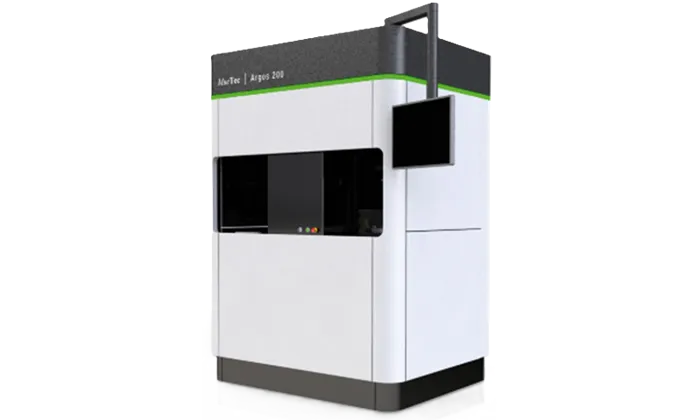
  • CD (Critical Dimension) Measurements:
    • CD measurement
    • Line Edge Roughness (LER)
    • Pattern measurement
    • Shading correction
  • Overlay (OVL) Metrology:
    • Box-in-box
    • Frame-in-frame
    • L-bars
    • Circle-in-circle
    • Custom overlay features
  • Infrared (IR) Applications:
    • Sealing inspection after bonding (eutectic or glass frit bonding)
    • Device inspection after bonding
    • Overlay metrology after bonding
    • Critical dimension metrology after bonding

Argos 200

Use the arrow keys to navigate between tabs

MueTec’s Macro Defect Inspection systems are designed to support a wide variety of wafer types without the need for complex configuration. These systems are user-friendly and require no recipe creation, allowing for seamless operation. Designed to perform 100% inspection during the lithography process, they deliver throughput equal to or faster than typical lithography clusters. This enables customers to transition from sample-based and manual inspections to a fully automated, statistically reliable inspection workflow.

Key Features

  • Simultaneous brightfield and darkfield inspection on both frontside and backside of wafers
  • Optimized wafer handling system delivering up to 200 wafers per hour
  • No recipe required, ensuring ease of use and quick setup
  • Defect Inspection
  • Simultaneous brightfield and darkfield inspection on both the front and back sides of wafers, providing comprehensive defect detection across a wide range of surface conditions and wafer types.

Global Service

Location Detail

Social Media

Interactive Online

Contact Us

Leave Your Message

Affiliates

China | USA | Europe

Visiting Application

Visitor Portal

Vendor Management

Vendor Portal

About Us
Profile
Core Values
Contact Us
Product & Service
Representative
Own-Branding
Wafer Reclaim
ESG
Chairman's Words
Stakeholders
Reports
Careers
Development
Welfare
Job Search
Investors
Monthly Revenue
Annual Reports
Conference
Press Center
Latest News
Events
Newsletter

Copyright ©SCIENTECH. All trademarks and images are the property of their respective owners and protected by law.