Skip to header

Main navigation

辛耘公司 SCIENTECH SCIENTECH
      • Profile
      • Core Value
      • Organization
      • ESG
      • Inclusive Workplace
      • Certificates
      • Public Relations
      • Global Presence
      • Product List
      • Camera Lens
      • Wet Bench
      • Single Wafer
      • Advanced Baking
      • Release Layer Coating
      • Batch Panel-level Wet Process
      • Single Panel-level Wet Process
      • Glass Release Layer Coating
      • Temporary Bonding
      • Debonding & Cleaning
      • Debonding
      • 12" Wafer Reclaim
      • Message from the Chairman
      • ESG Committee
      • Stakeholders
      • Materiality Issues
      • Integrity and Pragmatism
      • Supportive Workplace
      • ECO friendly
      • Social Contribution
      • GHG Emissions
      • Photo Gallery
      • ESG Report
      • Welfare
      • Job Search
      • Learning and Development
      • Fundamentals
      • Annual Reports
      • Monthly Revenue
      • Board of Directors
      • Committees
      • Internal Audit
      • Risk Management
      • Major Internal Policies
      • Status Report
      • Shareholders' Meeting
      • Investor Conference
      • Stock Quotes
      • TWSE MOPS
      • Contacts
      • Latest News
      • Event List
      • Newsletter
  • English
  • 繁體中文
SCIENTECH

HPSP

Breadcrumb

  • Home
  • HPSP

HPSP (High Pressure Solution Provider) is a leading Korean equipment manufacturer specializing in high-pressure annealing technologies for the global semiconductor industry. Its flagship product is a vertical furnace engineered for advanced high-pressure anneal processes.

HPSP pioneered the world's first and only H2/D2 high-pressure anneal technology. This breakthrough addresses critical challenges in advanced node manufacturing for both logic and memory applications.

Beyond its core annealing technology, HPSP operates a robust global sales and service network across the United States, Europe, and Asia, offering comprehensive customer support throughout the semiconductor value chain.
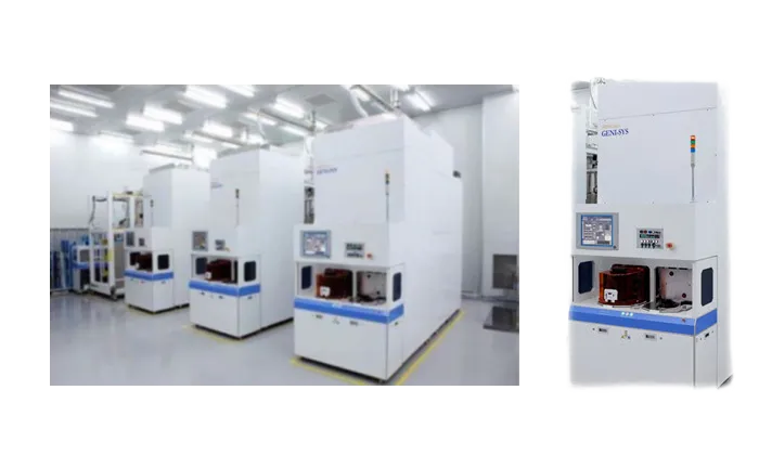
GENI-SYS

Use the arrow keys to navigate between tabs

The GENI-Sys System is a vertically oriented, high-pressure, fully automated thermal processing furnace designed for 200 mm and 300 mm wafer applications. Engineered to meet the semiconductor industry's latest standards for equipment design, cleanliness, manufacturing, and process control, the GENI-Sys ensures reliable performance in demanding manufacturing environments.

Capable of processing at up to 25 ATM, this system delivers exceptional annealing effects at temperatures below 450°C, making it ideal for applications where thermal budget constraints are critical.

Key Features
  • Supports 200 mm or 300 mm wafers with cassette loading configuration
  • Dry gas operation is standard; optional steam environment available
  • Flexible wafer handling for front-side or back-side processing
  • External boiler available for wet process requirements
  • Provides a solution for CMOS device improvement including high-k, metal gate, and various metal silicides.
  • High temperature (500-1100°C) highest growth rate for thick oxides application for various devices, such as, MEMS, Solar Cell, Optoelectronics, FPD, etc..
  • Designed for advanced thermal processing, such as various oxide layers, using a variety of gases and/or steam.
  • Temperatures are programmable and controllable from 150 to 1100 °C for both low and high temperature processes.
  • Process pressures range from 1 to 25 atmospheres. Wafers can be processed in either a dry gas or steam environment.
  • SEMI-S2
  • ANSI Z535.4 and/or ISO 3864.2

Global Service

Location Detail

Social Media

Interactive Online

Contact Us

Leave Your Message

Affiliates

China | USA | Europe

Visiting Application

Visitor Portal

Vendor Management

Vendor Portal

About Us
Profile
Core Values
Contact Us
Product & Service
Representative
Own-Branding
Wafer Reclaim
ESG
Chairman's Words
Stakeholders
Reports
Careers
Development
Welfare
Job Search
Investors
Monthly Revenue
Annual Reports
Conference
Press Center
Latest News
Events
Newsletter

Copyright ©SCIENTECH. All trademarks and images are the property of their respective owners and protected by law.