Micro Bump Technology for Advanced Packaging
1. Introduction
Micro bumps are critical miniature solder interconnects used in advanced packaging technologies. Their size is typically below 40 μm, and can even shrink to 10–20 μm, which is significantly smaller than traditional BGA (diameter > 500 μm) or flip chip bumps (diameter ~80–120 μm). They are used to enable high-density interconnections between die-to-die or die-to-interposer.
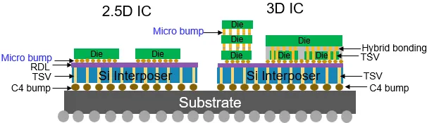
As chip functionality becomes increasingly complex and Moore’s Law approaches its physical limits, the semiconductor industry has shifted its focus from pure transistor scaling to packaging innovation. The industry is gradually transitioning from monolithic SoC (System-on-Chip) designs to chiplet and heterogeneous integration architectures. To achieve high-density interconnects between chips, micro bump technology has been widely adopted in 2.5D / 3D and chiplet packaging.
2. Micro Bump Structure
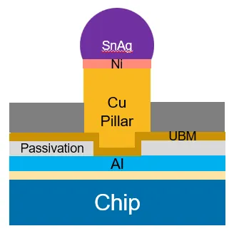
Micro bumps are often combined with underfill for reliability enhancement. A micro bump typically consists of the following layers (from bottom to top):
- UBM (Under Bump Metallization): Usually composed of titanium (Ti) and copper (Cu), responsible for enhancing adhesion and preventing atomic diffusion.
- Cu Pillar: The main body of the bump, providing excellent electrical conductivity and mechanical support while enabling pitch shrinkage for high-density packaging.
- Barrier Layer: Typically nickel (Ni), used to prevent excessive reaction between copper and tin, which would otherwise form overly thick and brittle intermetallic compounds (IMC).
Solder Cap (e.g., SnAg): Typically a lead-free tin-silver alloy (SnAg). After reflow heating, it bonds with the metal pad of the opposing chip.
3. Functions of Micro Bumps
The primary function of micro bumps is to serve as electrical interconnections and mechanical support between die-to-die or die-to-interposer structures.
- Die-to-Die Interconnect
Commonly used in HBM memory stacking and chiplet architectures:
- Provide high-density I/O
- Shorten signal transmission distance
- Reduce RC delay and power consumption
- Increase data bandwidth
- Die-to-Interposer Interconnect
- Support integration of chips fabricated at different process nodes (chiplet architecture)
- Connect logic chips, memory chips, analog modules, and RF modules
4. Major Applications of Micro Bumps
Compared with traditional bumps, micro bumps are characterized by high density, fine pitch, and high I/O count.
- 2.5D Packaging (Die-to-Interposer Connection)
- Features: Multiple dies mounted on a silicon interposer; provides high-density routing.
- Applications: High-Performance Computing (HPC), AI accelerators.
- 3D IC Vertical Stacking (Die-to-Die Connection)
- Functions: Used together with TSV (Through-Silicon Via); enables vertical die stacking; improves integration level and performance; reduces package footprint.
- Applications: HBM memory stacking, CMOS image sensors (CIS), mobile SoC chips.
- Chiplet Architecture
- Advantages: Connects different functional dies via micro bumps; improves design flexibility; increases yield; reduces manufacturing cost.
- Applications: CPU and I/O die separation; heterogeneous integration (Logic + RF + Analog); partitioned design of large AI chips.
5. Challenges of Micro Bumps
As line width and spacing shrink below 20 μm, technical challenges become increasingly significant:
- Scaling Limitations: Reduction in solder size accelerates the formation of Intermetallic Compounds (IMC), leading to decreased joint strength and compromised electrical conductivity.
- Electromigration (EM): High current densities in small volumes trigger electromigration, forming voids that result in open or short circuits.
- Process Cost and Yield: Heightened requirements for lithography precision and plating uniformity necessitate expensive advanced equipment (steppers/PVD). High-density interconnects are also extremely sensitive to defect density.
6. Future Development Trends
- Continuous Scaling: Moving from 40 μm down to 20 μm, and eventually reaching sub-10 μm to meet AI/HPC demands.
- Hybrid Bonding: As dimensions shrink below 10 μm, micro bumps may be replaced by Hybrid Bonding due to its solder-less nature, lower RC delay, and better thermal conductivity.
- Direct Cu-to-Cu Bonding: Reduces contact resistance and improves signal integrity for high-frequency applications.
7. Conclusion
Micro bumps are a pivotal technology in advanced packaging, enabling high-density interconnects for 2.5D/3D ICs and Chiplets. While facing challenges in scaling, reliability, and cost, they remain the dominant solution for the industry. In the coming years, while Hybrid Bonding and Cu-Cu bonding emerge, micro bumps will continue to be a mainstay in advanced semiconductor integration.


