Skip to header

Main navigation

辛耘公司 SCIENTECH SCIENTECH
      • Profile
      • Core Value
      • Organization
      • ESG
      • Inclusive Workplace
      • Certificates
      • Public Relations
      • Global Presence
      • Product List
      • Camera Lens
      • Wet Bench
      • Single Wafer
      • Advanced Baking
      • Release Layer Coating
      • Batch Panel-level Wet Process
      • Single Panel-level Wet Process
      • Glass Release Layer Coating
      • Temporary Bonding
      • Debonding & Cleaning
      • Debonding
      • 12" Wafer Reclaim
      • Message from the Chairman
      • ESG Committee
      • Stakeholders
      • Materiality Issues
      • Integrity and Pragmatism
      • Supportive Workplace
      • ECO friendly
      • Social Contribution
      • GHG Emissions
      • Photo Gallery
      • ESG Report
      • Welfare
      • Job Search
      • Learning and Development
      • Fundamentals
      • Annual Reports
      • Monthly Revenue
      • Board of Directors
      • Committees
      • Internal Audit
      • Risk Management
      • Major Internal Policies
      • Status Report
      • Shareholders' Meeting
      • Investor Conference
      • Stock Quotes
      • TWSE MOPS
      • Contacts
      • Latest News
      • Event List
      • Newsletter
  • English
  • 繁體中文
SCIENTECH

SURUGA SEIKI

Breadcrumb

  • Home
  • SURUGA SEIKI

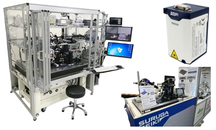
SURUGA SEIKI Co., Ltd., founded in 1964, has been a leading provider of high-quality, competitive products in the optical machinery market for over 50 years. In response to demands for quality control, cost reduction, and increased production, Suruga Seiki has accumulated advanced manufacturing technologies and remains committed to innovative product development. Its durability and reliability have earned top recognition across industries, making it the No. 1 brand in sales volume in Japan.

Suruga Seiki manufactures both automatic and manual precision linear stages. Its Laser Auto Collimators are renowned for high precision, non-contact measurement, instant evaluation, and the smallest form factor in the industry.

Tailored solutions are provided to meet specific customer requirements, including:

  • Probe card positioning technology
  • Precision enhancement solutions for wafer exposure systems
  • High-speed wafer transfer alignment modules

Global Service

Location Detail

Social Media

Interactive Online

Contact Us

Leave Your Message

Affiliates

China | USA | Europe

Visiting Application

Visitor Portal

Vendor Management

Vendor Portal

About Us
Profile
Core Values
Contact Us
Product & Service
Representative
Own-Branding
Wafer Reclaim
ESG
Chairman's Words
Stakeholders
Reports
Careers
Development
Welfare
Job Search
Investors
Monthly Revenue
Annual Reports
Conference
Press Center
Latest News
Events
Newsletter

Copyright ©SCIENTECH. All trademarks and images are the property of their respective owners and protected by law.