Camtek is a leading provider of advanced inspection and metrology solutions for the semiconductor industry. Its systems support the entire semiconductor production flow—from front-end and mid-end processes to post-dicing inspection and metrology. Designed to serve high-demand segments such as Advanced Interconnect Packaging, Memory, CMOS Image Sensors, MEMS, and RF, Camtek’s tools help ensure optimal yield and performance. Camtek serves top-tier IDMs, OSATs, and foundries globally through its subsidiaries in the US, Europe, Japan, China, Hong Kong, Taiwan, Korea, and Singapore. Its platforms deliver reliable high-throughput defect detection, ensuring that only known-good-die proceed to final products. With the growing adoption of advanced packaging technologies, Camtek offers customizable inspection and metrology solutions that meet the industry’s highest quality standards while supporting rapid production scaling and faster time to market.
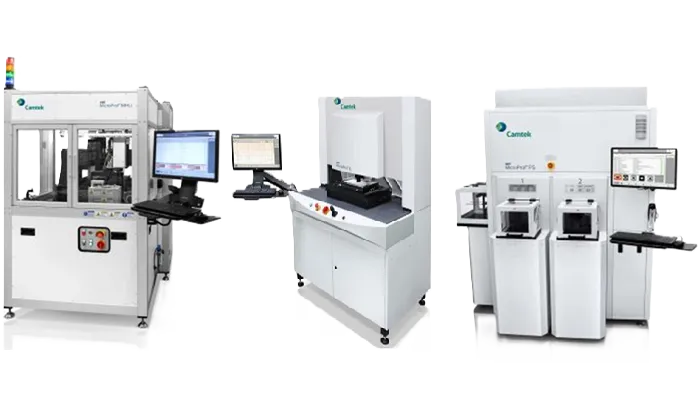
The FRT MicroProf series is a high-precision metrology solution designed for the semiconductor industry, enabling comprehensive geometric measurements of wafers, including thickness, TTV (Total Thickness Variation), Bow, Warp, TIR (Total Indicated Runout), and LTV (Local Thickness Variation). Utilizing a white light source and a dual-probe configuration (top and bottom), the system performs non-contact measurements by positioning the wafer between the probes, allowing for efficient and accurate analysis in a single pass.
An optional infrared (IR) probe enhances measurement capabilities by enabling penetration of materials like silicon (Si) and gallium arsenide (GaAs), making it ideal for monitoring thickness changes during the backside thinning process. The system supports both manual and automated configurations to meet varying production needs.
- Standard fixture supports samples from 2 to 12 inches
- Measures thickness, TTV, Bow, and Warp on opaque and transparent materials
- Optional IR probe for non-destructive layer thickness measurement on Si/GaAs
- Ideal for incoming inspection, EPI process monitoring, and thinning process control
- Available in manual (MicroProf 200/300) and automated (MicroProf 200/300 MHU) models
- Integrated mapping function for multi-point measurement and wafer map generation
- Built-in reference wafers for fast and accurate thickness calibration


