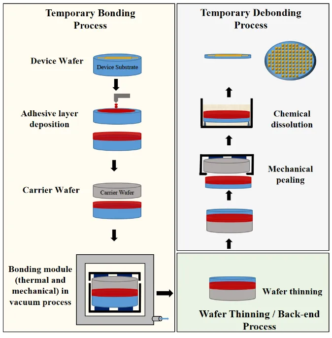
Efficient management of the substrate has been a key factor in the progress of modern electronic civilization, enabling the creation of compact high-performance devices. The development of 3D IC stacking has been facilitated by the reduction in substrate thickness, which allows several ICs to be squeezed and stacked as a single package. However, handling ultrathin wafers and reducing wafer thickness without damaging the pre-process has been a challenging task for semiconductor industries. Temporary bonding and debonding (TBDB) technology was developed to address this. TBDB technology involves temporarily bonding a device wafer to a carrier wafer using an intermediate material, which provides physical stability for thin wafers or wafers to be trimmed during processing. This allows the delicate device wafer to be processed with additional mechanical support. The wafer stack is debonded once the necessary processing steps are completed, as explained in Figure.
Continuous progress and development in TBDB technology have increased the yield and productivity of ultra-thin device production, and further advancements in TBDB efficiency and quality could greatly enhance the market competitiveness of advanced packaging. Novel temporary bonding materials and improved TBDB techniques are crucial for overcoming technical challenges in high-end chip thinning procedures and would directly contribute to the rapid development of advanced packaging. This technology provides solutions for ultra-thin wafer processing and handling, ultra-thin device manufacturing, and 3D stacked packaging systems.
One of the main advantages of TBDB technology is that it enables the processing of flexible substrates on existing semiconductor manufacturing equipment, which is not typically designed for the processing of flexible materials. The technology also allows for the manufacture of ultra-thin flexible electronic components, which are essential for wearable devices and other applications where thinness and flexibility are critical.
Scientech is a well-established semiconductor equipment merchandiser with over 40 years of experience, including over 15 years of expertise in developing and manufacturing precision packaging equipment and wafer bonding solutions. Our flagship wafer bonding equipment is highly regarded in the industry for its ability to produce high volumes of precision bonding and can be tailored to meet individual manufacturing needs. The equipment is equipped with a highly accurate aligner that can achieve precision up to 5 µm and notch accuracy of 0.1degree. To ensure that the required adhesive thickness fifty sampling points are studied on a single wafer.
Our bonding process uses a dual approach, combining both thermal and mechanical methods, to ensure that the bonding is done with the utmost integrity. The bonding process is executed in a vacuum atmosphere to eliminate air bubbles and utilize a tunable temperature module to achieve optimal results. Additionally, warpage caused by load pressure is eliminated, as we apply extremely low load pressure of less than 1 mtorr. This guarantees that our bonding process is of high quality and meets the required standards.
Our system has a high degree of adaptability, which allows it to be used for a variety of post-processing applications such as solder ball mounting and fan-out wafer-level packaging (FOWLP). Overall, our system's adaptability makes it an excellent choice for a wide range of post-processing applications, enabling us to meet the needs of our customers in various industries.
At Scientech, we are dedicated to providing exceptional products and services as a premier semiconductor equipment manufacturer and supplier based in Taiwan. Our commitment to excellence ensures that our customers receive only the highest quality products and services.


