半導體公司在建置廠房與採購設備時,往往需投入龐大的資本,使半導體產業成為高度資本密集型產業。為了維持競爭力並持續跟進最新技術節點,半導體公司必須不斷尋求創新方式,在不影響技術品質與設備效能的前提下,最佳化支出結構並降低資本支出(CAPEX)。
在半導體產業中,降低資本支出的關鍵之一在於有效提升設備使用效率。透過針對實際製程需求進行設備設計,可避免不必要的設備投資。此外,製程最佳化亦扮演重要角色,可藉由縮短 cycle time、提升良率及降低耗損,全面提升製程效率。透過上述作法,半導體公司得以在達成既定製造目標的同時,有效控管資本支出。
另一方面,將非核心業務(如製程設備的設計與製造)委外予具專業能力的第三方設備供應商,有助於降低自建設備與產線所需的高額成本。委外合作亦可導入外部專業技術與製程經驗,提升整體產品與服務品質。透過跨公司合作與策略夥伴關係,亦可加速新技術導入,特別有助於新創或成長中企業縮短技術學習曲線。
透過持續的製程改善,半導體公司可進一步降低資本支出。常見作法包括不斷精進製造流程以提升效率並減少浪費,並導入如 Six Sigma 等方法論,以降低缺陷率並強化品質穩定度。
在高資本支出壓力與激烈競爭並存的環境下,半導體產業必須同時兼顧投資效率與技術領先。前述策略,包括設備最佳化、委外合作、跨界夥伴關係、精實製造與製程改善,皆有助於在持續投資先進技術與設備的同時,有效降低整體支出,進而提升營運效率與獲利能力。
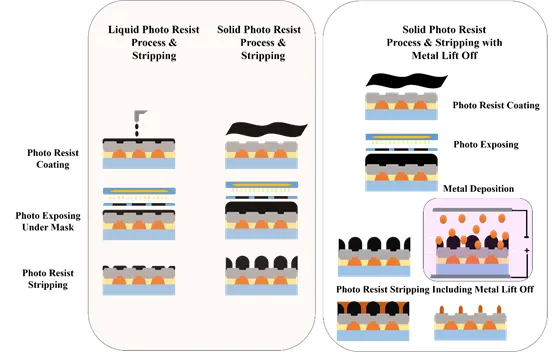
在現代半導體製程中,光阻剝離(Photoresist Stripping)為關鍵製程步驟之一。於微影製程完成後,需將曝光後的光阻自晶圓表面移除,以顯露已形成圖形的區域,供後續製程進行。
隨著製程節點持續微縮,主動區尺寸不斷縮小,微影製程複雜度顯著提升,圖形線寬與間距更加緊密,使光阻剝離作業面臨更高挑戰。剝離過程需在不損傷基板或已形成圖形結構的前提下完成,對製程控制提出更高要求。
Scientech 為深耕半導體設備產業逾 40 年的專業設備供應商,並具備超過 15 年精密封裝設備與晶圓鍵合解決方案的設計與製造經驗。Scientech 最新推出的 PR Stripper(浸泡+噴淋模組)採用混合式架構設計,兼具單片式製程的高品質控制能力與槽式製程的高產能優勢,可在單一設備中同時實現高良率與高產出。
此混合式 PR Stripper 可針對單片晶圓或特定批次晶圓進行製程監控與參數調控,並支援不同尺寸晶圓(如 8 吋與 12 吋)於同一設備中同時處理。透過長期製程研究與數據分析,Scientech 成功開發出可高效去除固態與液態膜狀光阻的剝離製程,在兼顧成本效益的同時,確保製程穩定性與品質表現,如圖所示。
於剝離過程中,化學藥液可溶解光阻與殘留物,並將不溶性金屬材料進行 lift-off。使用傳統 PR 剝離設備時,化學槽中殘留物與漂浮雜質的管理,往往對良率造成顯著影響。Scientech 的混合式 PR Stripper 透過專用浸泡槽設計,有效控制殘渣累積,並搭配雙重長效濾材,在維持高過濾效率的同時,降低化學藥液耗用。
此外,設備採用多組機械手臂進行乾、濕晶圓搬送,有效避免交叉汙染。完成浸泡製程後,晶圓將進入噴淋模組,依序進行剝離藥液、異丙醇(IPA)、去離子水(DI Water)清洗,並以高溫氮氣進行乾燥。所有噴淋模組皆具備可調式噴灑壓力與時間控制機制,可依不同製程需求進行最佳化設定。
Scientech 的核心優勢,在於能依據每一位客戶的實際製程需求,提供高度客製化的設備設計與解決方案。Scientech 的 PR Stripper 採用高度可程式化模組設計,可彈性調整浸泡與噴淋製程參數,使單一設備即可對應不同厚度光阻的剝離需求,滿足多元製程應用。


