三維積體電路(3DIC)已成為因應現代應用對高效能與高整合度需求的重要解決方案。透過將多顆晶片或晶圓堆疊為單一封裝,3DIC 技術相較於傳統二維(2D)積體電路,具備多項顯著優勢。
3DIC 的關鍵特性之一在於晶圓厚度的持續薄化。藉由垂直堆疊多層晶片,可大幅縮小整體電路占用面積,相較於平面式 2D 佈局,能實現更高的電路密度,並在有限空間內整合更複雜的功能。另一項核心需求則是堆疊晶片之間的高效互連。互連技術對於積體電路效能至關重要,負責不同元件與層級之間的訊號傳輸。在 3DIC 中,主要互連技術包含穿矽通孔(Through-Silicon Via, TSV)與焊錫凸塊(Solder Bump)。TSV 提供垂直方向的電性連接,而焊錫凸塊則負責晶片或晶圓堆疊間的實體與電性連結。
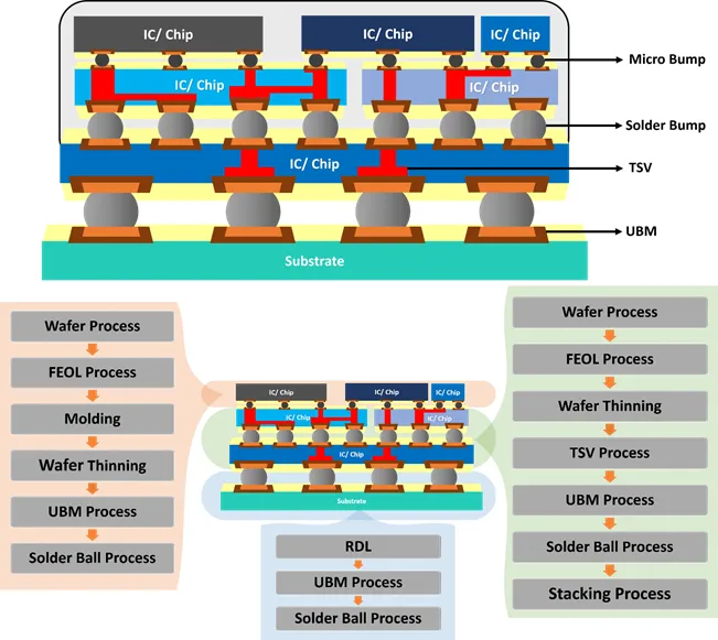
以下為 3DIC 製造流程之概述。晶圓前處理:包含清洗、檢測與對位。前段製程(FEOL):於基礎晶圓上製作主動元件,如電晶體與邏輯電路。晶圓薄化:透過支撐系統對已完成製程之晶圓進行研磨與薄化,以降低整體厚度。TSV 製作:形成穿越矽基板的垂直互連結構。UBM 製作:於互連表面形成 Under-Bump Metallization(UBM)層,提供焊錫凸塊與晶片之間穩定的電性與機械連結。典型 UBM 結構由多層金屬組成,例如鈦(Ti)、鎢(W)與銅(Cu)。焊錫凸塊形成:透過回焊(Reflow)或焊錫球植球等方式形成凸塊,作為堆疊晶片間的實體互連。重新佈線層(Redistribution Layer, RDL):主要功能為連接 PCB 或其他 IC。晶片堆疊:將薄化後的晶圓進行對位並堆疊,使 TSV 與焊錫凸塊精準對齊,並透過直接鍵合或膠合等方式完成接合。封裝:使用模封材料或底填膠進行結構保護,並將外部接點連結至焊錫凸塊,以實現電性存取。整體製程流程如圖所示。
在 3DIC 中導入焊錫球互連時,可能面臨原子遷移與金屬間化合物反應等問題,進而導致空洞形成並影響電性效能。為解決上述挑戰,可透過 Under-Bump Metallization 製程沉積阻障層,有效抑制原子遷移與金屬間反應,進而提升焊錫互連的可靠度與效能。UBM 製程在 3DIC 技術中扮演關鍵角色,不僅可確保電性連接穩定性、提升機械強度、抑制不良反應,亦能精準控制凸塊尺寸與形貌,整體有助於提升 3DIC 封裝的效能、可靠度與量產可行性。
Scientech 長期支援多項半導體製造製程,協助實現晶片薄化並提升整體效能。在 3DIC 應用領域中,Scientech 提供完整的半導體製程設備解決方案,包含暫時鍵合與解鍵合(Temporary Bonding/Debonding)、電鍍(Electroplating)、雷射回焊植球(Laser Reflow Ball Mounting)、濕蝕刻(Wet Etching)、焊錫球蝕刻(Solder Ball Etching)及 UBM 蝕刻等。其中,Scientech 的 UBM 蝕刻設備憑藉高度客製化能力與高精度製程控制,廣受產業客戶採用。
UBM 蝕刻設備可依需求提供多種模組配置,包括僅具噴淋蝕刻(Spray Etching)的單片式設備,以及結合噴淋與浸泡功能的機型,可有效強化亞微米級腔體蝕刻能力。透過精細化製程調校,該設備可在兼顧品質與成本效益的前提下,穩定產出高品質蝕刻成果。
此外,透過製程整合設計,可將光阻剝離(PR Stripper)、金屬 Lift-off 與 UBM 蝕刻整合於同一設備或製程平台中。此種整合式製程策略可有效縮短製程時間、降低設備投資與製造成本,進一步提升 3DIC 製造的整體競爭力。


