半導體產業對品質與製程精度的高度要求,來自於不斷演進的技術節點需求以及全球市場的高度競爭。唯有在半導體設計與製造的各個環節中,持續維持嚴謹的品質標準,才能確保產品具備高可靠度與高效能。半導體品質與測試流程及品質控管機制密切相關,測試晶圓(Test Wafer)在半導體製程的每一階段皆需經過嚴格檢測與驗證,於製造、失效分析與品質保證中扮演不可或缺的角色。測試晶圓對於確保半導體元件與技術的可靠性與製程效率,具有關鍵性的重要地位。
在典型的 CMOS 邏輯與記憶體製程中,每一批次晶圓中所配置的測試晶圓比例,通常約占該批次總晶圓數的 10% 至 20%。實際比例會依半導體製造商所採行的品質控管策略,以及製程複雜度而有所不同。
此外,透過測試晶圓回收再生(Wafer Reclaim),可作為採購新晶圓以外的具成本效益替代方案。此作法已成為現代半導體製程中不可或缺的一環,不僅同時符合經濟效益與環境永續目標,也有助於持續推動半導體製造流程的改善與技術創新。
一般而言,晶圓回收製程包含以下主要步驟:初步檢測、分類、回收處理、最終拋光以及缺陷檢查。首先,需對待回收晶圓進行全面檢測與分類。晶圓分類是回收製程中極為關鍵的一環,因其將決定後續所需採用的回收流程。不同製程條件下,具圖形與無圖形晶圓,以及未鍍膜與已金屬鍍膜晶圓,皆需依其材料與化學特性進行對應分類與製程規劃。
Scientech Corporation 為深耕半導體設備產業多年的台灣專業供應商,累積超過 40 年產業經驗,並具備逾 15 年的設備設計與製造實績。同時,Scientech 亦持續提供高品質的晶圓回收服務超過 17 年,並隨著產業需求不斷精進其製程與技術能力。
Scientech 於回收作業初期,會依不同晶圓條件進行嚴謹分類,並針對各類別晶圓採用專屬且最佳化的回收製程方案。其技術能力可完整支援矽(Si)與碳化矽(SiC)晶圓,無論是否具備圖形結構,亦不論為金屬鍍膜(如銅、銀)或非金屬鍍膜晶圓,皆能提供對應的回收處理能力。
其中,針對銅鍍膜晶圓,Scientech 採取獨立製程線進行處理,以因應其特殊化學特性,並有效降低交叉汙染風險。每片晶圓皆需經過多道濕式化學剝離製程,以去除圖形結構、表面鍍膜材料及外來缺陷。隨後進行最佳化調校之拋光製程,精準去除受控厚度的矽材料,使晶圓正反兩面(視需求)皆達到目標規格。拋光完成後,所有晶圓皆會經過 RCA 清洗流程與高效乾燥處理,以確保其潔淨度符合後續製程使用需求。
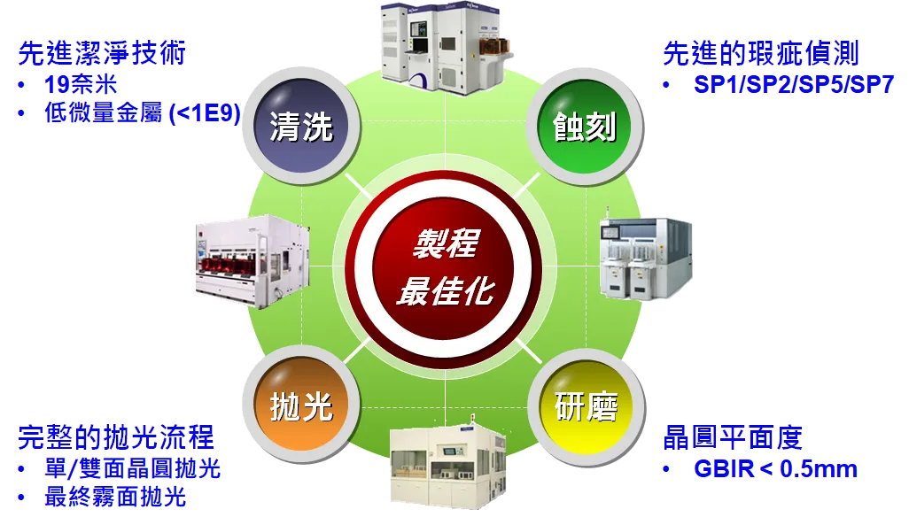
最後,所有回收完成之晶圓皆需進行嚴格的最終檢測,以確認是否存在物理性損傷,並量測表面粒子尺寸,確保符合最高等級的品質控管標準。其中,粒子尺寸管理為晶圓回收製程中極為關鍵的指標。Scientech 的晶圓回收製程可穩定達成 26–19 nm 的粒子尺寸控制範圍(對應 5 nm 技術節點需求),同時將金屬殘留濃度控制於 1E9 以下,並實現表面粗糙度 GBIR 小於 0.5 μm 的優異表現。此外,其月產能可超過 160,000 片晶圓,充分展現 Scientech 在兼顧高品質與高產能方面的實力,持續為半導體品質提升提供堅實支援。


