PacTech is a technology-driven company specializing in advanced packaging equipment and wafer-level packaging services. Since its founding, PacTech has focused on developing next-generation technologies for emerging applications.
Renowned for its flexibility in customization and unique solutions, PacTech’s team of experts actively addresses industry packaging challenges to deliver cost-effective, time-efficient, and innovative solutions.
The company is headquartered in Nauen, Germany, with additional manufacturing and operations facilities in Santa Clara, California, USA, and Penang, Malaysia.
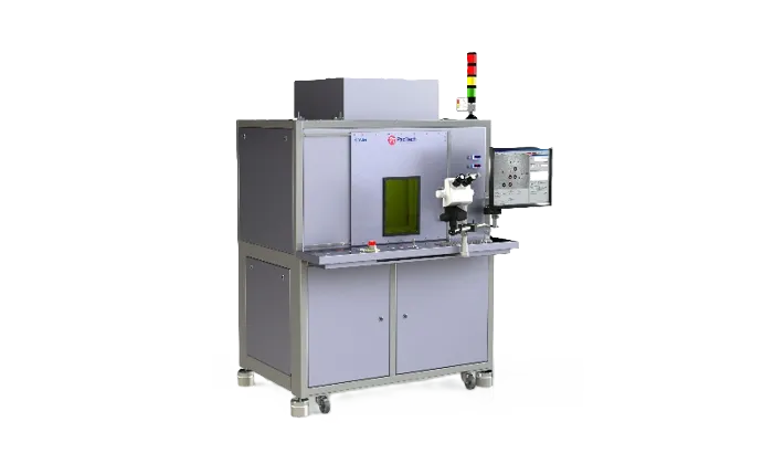
SB2 series–Laser Solder Jetting Equipment
The SB2 series offers a clean, precise, and flexible laser solder jetting solution. A singulation disc dispenses one solder ball into a capillary, where a laser melts it, allowing accurate placement and instant reflow on the target area. Compatible with various solder alloys and requiring no flux, the process is clean and reliable.
Laser-generated localized heat and short pulses ensure minimal thermal stress outside the bonding zone. The single-ball dispensing system is tool-free, allowing flexible, contactless soldering at any location.
Key Features
- Fluxless
- Mask/Stencil-free
- Clean process
- High placement accuracy
- Contactless soldering
- In-situ reflow with minimal thermal stress
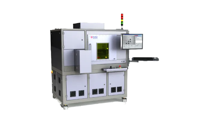
LaPlace – Laser Soldering and Assembly Equipment
Using localized laser heating, temperature is selectively applied to targeted interconnection areas without raising the entire substrate to reflow temperature—ideal for reflowing micron-scale interconnects. Through customized bond tools and laser technology, pick-and-place and reflow heating are achieved in a single, highly accurate step (<5µm).
This localized approach enables reliable bonding of large dies and supports ultra-small die assembly down to 300µm. LaPlace’s unique temperature control prevents overheating of chips or components and avoids substrate warpage or repeat reflow damage.
Key Features
- Localized, selective laser heating
- Flexible laser beam shaping
- High placement accuracy
- Compatible with materials with CTE mismatch
- Customizable bond tools
- In-situ reflow with minimal thermal stress


