Three-dimensional integrated circuits (3DICs) have emerged as a promising solution to meet the increasing demands for high performance and compactness in modern applications. By stacking individual ICs/wafers together as a single package, 3DIC technology offers several advantages over traditional two-dimensional (2D) integrated circuits.
One of the key characteristics required for 3DICs is the reduction in wafer thickness. By stacking multiple layers vertically, the overall footprint of the circuit can be significantly reduced compared to a planar 2D layout. This enables higher circuit density and allows for more complex functionality within a smaller space. Another crucial requirement of 3DIC technology is the effective interconnect between the stacked ICs. Interconnects play a vital role in determining the performance of integrated circuits, as they enable communication between different components and layers. Interconnect technologies in 3DICs are Through-silicon vias (TSVs) and soldier bumps. TSVs are utilized to provide vertical connections within a stacked IC, solder bumps physically connect and communicate between the stacked ICs or chips.
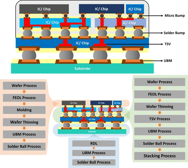
A brief overview of the process flow for manufacturing 3DIC. Wafer Preparation: Involves cleaning, inspecting, and alignment. Front-end-of-Line (FEOL) Processing: the process involves the fabrication of active devices, such as transistors and logic circuits, on the base wafer. Wafer Thinning: The processed wafer is thinned to reduce the overall thickness through the wafer support system. TSV Formation: TSVs are vertical interconnects that pass through the silicon substrate. UBM Formation: UBM layer is formed on the surface of interconnects. The UBM layer provides a reliable electrical and mechanical connection between the chip and the solder bumps. A typical UBM layer consists of multiple metal layers, such as titanium (Ti), tungsten (W), and copper (Cu). Solder Bump Formation: Typically using techniques like solder reflow or solder ball placement, to create the solder bumps. These bumps will serve as the physical interconnections between the stacked ICs. Redistribution Layer (RDL): The primary function of the RDL is to connect with other devices, such as a printed circuit board (PCB) or another IC. Stacking: The thinned wafers are then stacked or bonded together, aligning the TSVs and the solder bumps on each layer. The stacked wafers are bonded using techniques such as fusion bonding or adhesive bonding. Packaging: Packaging processes involves encapsulating the 3DIC structure with protective materials, such as molding compounds or underfills, and connecting the external leads or pins to the solder bumps for electrical access. The overview of the process flow sequence is represented in Figure.
The implementation of solder balls in 3DICs can encounter significant drawbacks, including atom migration and intermetallic reactions that can lead to void formation and adversely impact electrical performance. To address these challenges, a viable strategy involves the deposition of barrier layers through under-bump metallization. This approach effectively mitigates the detrimental effects of atom migration and intermetallic reactions, resulting in enhanced reliability and performance of solder ball-based interconnects in 3DICs. The UBM process is important in 3DIC technology as it enables reliable electrical connections, enhances mechanical integrity, prevents intermetallic reactions, and controls bump shape and size. These factors collectively contribute to the performance, reliability, and manufacturability of 3DIC packages, facilitating the integration of multiple chips or dies in a compact and efficient manner.
Scientech plays a vital role in supporting a wide range of manufacturing processes in semiconductor technology, resulting in reduced thickness and enhanced performance. Specifically for 3DICs, Scientech offers various semiconductor process instruments, including temporary bonding and debonding, electro-plating, laser reflow ball mounting, wet etching, solder ball etching, and UBM etching. Among these tools, Scientech's UBM etching tool is highly popular in industries due to our expertise in customizing equipment to meet each client's unique needs with high precision. Additionally, the UBM etching tool is available in different modules, such as the single-wafer tool with only spray etching, and spray etching with immersion functionality which enhances the ability to etch the cavity below a micron. The ability to fine-tune processes for precise requirements has enabled the UBM etching tool to deliver high-quality work cost-effectively.
Furthermore, the tool's customization feasibility has led Scientech to play a vital role in supporting a wide range of manufacturing processes in semiconductor technology, resulting in reduced thickness and enhanced performance. Specifically for 3DICs, Scientech offers various semiconductor process instruments, including temporary bonding and debonding, electro-plating, laser reflow ball mounting, wet etching, solder ball etching, and UBM etching. Among these tools, Scientech's UBM etching tool is highly popular in industries due to our expertise in customizing equipment to meet each client's unique needs with high precision. Additionally, the UBM etching tool is available in different modules, such as the single-wafer tool with only spray etching, and spray etching with immersion functionality which enhances the ability to etch the cavity below a micron. The ability to fine-tune processes for precise requirements has enabled the UBM etching tool to deliver high-quality work cost-effectively.
To combine various processes, particularly integrating PR stripper, and metal liftoff with UBM etching. This combinational approach helps reduce manufacturing costs and processing time.


