繁體中文
繁體中文 English
Activities
| 2020/09 |
|
||||||||||||
| 2020/08 |
|
||||||||||||
| 2020/07 |
|
||||||||||||
| 2020/07 |
|
||||||||||||
| 2020/06 |
|
||||||||||||
| 2020/05 |
|
||||||||||||
Content changed at :2020-07-02 15:52:50
| 2020/09 |
|
||||||||||||
| 2020/08 |
|
||||||||||||
| 2020/07 |
|
||||||||||||
| 2020/07 |
|
||||||||||||
| 2020/06 |
|
||||||||||||
| 2020/05 |
|
||||||||||||
The increasing demand for electronic equipment is driven by factors such as the escalation of digital transformation, consumer electronics, IoT, automotive electronics, industrial automation, communication infrastructure, and emerging technologies. Semiconductors serve as the foundation for these technologies, enabling the development of advanced and interconnected electronic devices that cater to diverse industry needs.
Further, the semiconductor industry significantly contributes to economic growth and competitiveness. Mass production of semiconductors stimulates job creation, attracts investments, and enhances the competitiveness of nations in the global market. It strengthens the overall economy by driving innovation, supporting related industries, and generating revenue.
The accelerated usage of electronic devices and the ongoing digital transformation have indeed created a strong need to increase the mass production of semiconductors. However, a limited number of semiconductor companies are involved in producing the core technology. Increasing mass production and simultaneously maintaining the quality of fabrication can ensure the stability in global supply chain. Fabrication of semiconductor devices and ICs consists of numerous steps and processes involving wet and dry processes. Here is the general overview of the fabrication process, wafer preparation, cleaning, photolithography, developing, etching, cleaning, ion implantation, deposition, CMP, dicing, wire bonding, and packaging. The packaged devices are mounted onto circuit boards or other substrates, and they may undergo additional assembly steps to create the final electronic products, there are several more steps involved, along with various intricate technologies and techniques employed at each stage which may vary according to the requirements and products. Among these processes, several processes are categorized into dry and wet approaches. Further, the wet approach is classified as a single-wafer and bench process. The single-wafer process is highly used in FEOL for high precision but is time-consuming on the other hand wet bench process is highly used in BEOL for high yield and it conserves time. Etching, stripping, developing, and cleaning are considered to be highly crucial wet bench processes for semiconductor manufacturing. At present, wet bench technology has matured in dual aspects to deliver high yield while maintaining high precision.
Scientech’s wet process equipment has been successfully implemented in the fabrication of the recent chipset 3DIC, CoWoS and advanced packaging process. It has been incorporated into mass production, allowing customers to reap the benefits of this innovative packaging technique in a cost-effective approach. The ability to customize the equipment and interface led to fine-tuning the process for specific clients for certain tasks thus resulting in reducing the overall cost of ownership (CoO).
Scientech has established itself as a trusted partner in the semiconductor industry by offering reliable wet process equipment. Their expertise and innovative solutions contribute to the success of their customers in various segments of the semiconductor market.
If you have any further questions, please feel free to contact us by using Line or Email.
E-mail: info@scientech.com.tw
All the best!
Axus Technology Signs Scientech as Exclusive Distribution Partner for China and Taiwan, Expanding Global Footprint
Strategic Partnership Expedites Sales, Service and Support of Axus’s
CMP Processing and Cleaning Systems for Customers in Region
CHANDLER, Ariz., October 31, 2024 – Axus Technology, a leading global provider of chemical mechanical planarization (CMP) equipment, critical for semiconductor and compound semiconductor fabrication, today announced it has entered into a strategic distribution agreement with Scientech Corporation (Taipei, Taiwan). Scientech will now provide sales, installation, service, parts, process development assistance and technical support throughout China and Taiwan for Axus's Capstone CMP platform and Aquarius wafer-cleaning tools – designed specifically for processing complex compound semiconductor materials such as silicon carbide (SiC) and gallium nitride (GaN), as well as for other fast-growing markets such as advanced packaging.
In response to growing demand from key markets such as artificial intelligence (AI), renewable energy and automotive, compound semiconductor wafer production in the region is growing rapidly. According to Yole Group, China captured more than one-third of the SiC wafer and epi wafer market in 2023. Taiwan is also gaining notice for its government-funded program focused on gallium nitride epitaxial crystal growth on 200mm QST substrates (GaN-on-QST). These efforts heighten the need for capital equipment like Axus’s Capstone systems, which are optimized to meet these materials’ challenging process requirements.
“It’s exciting to see new development projects and applications in China and Asia that are creating new opportunities for compound semiconductors,” said Axus Technology CEO Dan Trojan. “Partnering with Scientech, which represents many well-known providers of capital equipment in the region, will ensure that customers have access not only to our product offerings but also to state-of-the-art service and support.”
“Axus Technology has demonstrated impressive success in building its customer base in North America and Europe,” said MT Hsu, CEO, Scientech Corp. “We look forward to helping the company expand its presence in Asia as demand for its high-performance, innovative CMP technology continues to accelerate.”
About Scientech Corporation
Scientech Corporation was established in 1979 and has headquarters in Taipei, Taiwan, with five additional offices across Taiwan and 10 offices in China. Scientech provides full sales, installation, service, parts, process development assistance and technical support for all representing equipment, tools and products. To learn more, visit www.scientech.com.tw
About Axus Technology
Led by its state-of-the-art Capstone® CMP and Aquarius™ wafer-cleaning platforms, Axus Technology is a recognized industry leader in designing and building modern, flexible next-generation equipment and providing custom process-development services. Axus enables companies of all sizes, from startups to high-volume manufacturers, to test, develop, and implement leading-edge solutions—particularly for novel and emerging materials—process integration schemes, products and applications. Axus’s equipment solutions range from low cost-of-ownership entry-level tools to state-of-the-art high-volume manufacturing systems. Process testing, development, optimization, and scaling are supported by our process applications lab and foundry, which includes a full array of process equipment and supporting metrology, and is staffed by the industry’s most experienced CMP team. For more information, visit www.axustech.com
Media Contacts:
Axus Technology Kiterocket
Emilie Marenec Lisa Gillette-Martin
T: 480-331-4981 T: 408-205-4732
E: emarenec@axustech.com E: lgmartin@kiterocket.com
ClassOne Signs Scientech as Rep for China, Taiwan and SE Asia
ClassOne Technology | March 8, 2017
Kalispell, Montana – ClassOne Technology (www.classone.com), manufacturer of wet processing equipment for 200mm and smaller wafers, announced that Scientech Corporation of Taipei, Taiwan, will become the company’s new representative for China, Taiwan and Southeast Asia, starting immediately.
Asia is an extremely active and important region for us," said Byron Exarcos, President of the ClassOne Group. "We wanted a respected and thoroughly experienced sales and support operation there, and Scientech filled the bill perfectly. They have all the necessary infrastructure and well-established field service teams, having served the industry for over three and a half decades — including many years representing Semitool. We’re proud and delighted to now have them on the ClassOne team.
We're very impressed by the rapid success ClassOne has been achieving, bringing high-performance wet processing solutions to the emerging markets — with more than 100 tools already installed across the U.S. and Europe," said M.T. Hsu, President of Scientech Corporation. “It's great to represent products that are in high demand, and we're looking forward to helping expand ClassOne's presence in Asia.
Scientech Corporation (www.scientech.com) was established in 1979 and has headquarters in Taipei, Taiwan, with five additional offices across Taiwan and Shanghai. Scientech will provide full sales, installation, service, parts, process development assistance and technical support for all ClassOne Technology equipment — including the Solstice® family of electroplating systems and the Trident® families of Spin Rinse Dryers and Spray Solvent Tools.
ClassOne stated that the company's mission is to provide advanced wet processing performance at an affordable price for users of 200mm and smaller substrates. Many of these users are in budget-limited emerging markets producing a range of devices such as MEMS, LEDs, RF, power and sensors. ClassOne's pricing is often less than half that of similarly configured 300mm systems outfitted for 200mm from the large manufacturers — which is why ClassOne tools have been described as delivering "Advanced wet processing for the rest of us."
The advancements in AI technology have indeed driven improvements in processing units, and these improvements often extend to the overall fabrication process of semiconductor devices. The demand for more powerful and efficient hardware to support AI workloads has led to the development of specialized accelerators. Graphics Processing Units (GPUs), Tensor Processing Units (TPUs), High Bandwidth Memory (HBM) and other custom-designed chips are being used to accelerate specific AI computations. The fabrication of these specialized chips involves advanced semiconductor manufacturing processes.
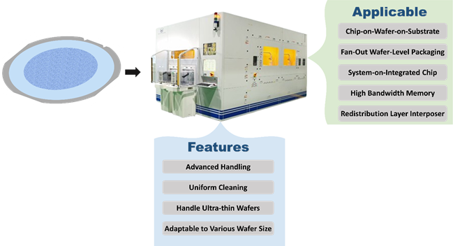
Further, AI applications often require a mix of processing units optimized for different tasks. Heterogeneous integration involves combining different types of processing units, such as CPUs, GPUs, and accelerators, on a single chip or package. 3D chip stacking technologies have paved the path for improved performance, reduced latency, and increased overall system efficiency. Chips are stacked using various advanced packaging technologies, allowing multiple semiconductor dies to be vertically integrated. Stacking chips in this manner offers important advantages. Some common methods for stacking chips: Chip-on-Wafer-on-Substrate, Fan-Out Wafer-Level Packaging, and System-on-Integrated Chip.
Handling and processing thin wafers mounted on a frame post-debonding, along with the subsequent cleaning process, presents formidable challenges in advanced semiconductor packaging technologies. Conventional cleaning methods carry the risk of damaging thinned wafers.
To navigate these complexities, Scientech Corporation, a Taiwan-based leading semiconductor equipment manufacturer, leverages cutting-edge solutions for wafer-on-frame cleaning. Advanced handling equipment and robotic systems, meticulously engineered for precision control, play a crucial role. These technologies reduce the risk of damage during handling and ensure that delicate wafers are treated with the utmost care. Scientech’s commitment to innovative solutions in semiconductor equipment highlights its dedication to addressing the unique challenges posed by handling and processing ultra-thin wafers after debonding.
Innovative cleaning techniques, specifically tailored to the unique characteristics of thin wafers, are deployed to enhance efficacy while minimizing potential harm. The ongoing development of specialized materials and processes further addresses challenges linked to the inherent flexibility, fragility, and intricate cleaning requirements of thin wafers mounted on frames post-debonding.
The continuous pursuit of technological advancements and the fine-tuning of processes are indispensable elements in the semiconductor industry's quest to improve yield and bolster the reliability of devices. Advantageous characteristics, the tool can handle various wafer sizes on a frame. Further, both the stand-alone wafer and wafer mounted on the frame can be processed in a single tool. These ongoing efforts are vital for mastering the intricacies of complex packaging processes and meeting the evolving demands of semiconductor manufacturing.
If you have any further questions, please feel free to contact us by using Line or Email.
E-mail: info@scientech.com.tw
All the best!
December 2022 Press Release
With the rapid development of the electronics industry, new applications such as AR, IoT, and HPC demand more and more advanced technology. In order to achieve smaller feature size, energy saving, high efficiency and low cost, the complexities of design and process increase significantly for each technology nodes, and then slowing down the Moore's Law. Therefore, the adoption of heterogeneous stack packaging technology will become crucial for Moore's Law continuity.
Being a leading semiconductor equipment and wafer reclaim supplier in Taiwan, Scientech Corporation has launched the development of wet process equipment in 2003. Scientech has successively supported customers in LED, Mini/Micro LED, compound semi and power components such as IGBT, SiC and GaN industries, as well as advanced packaging process such as Bumping, Fan-out, Chip-On-Wafer and so on. Our wet process equipment has been successfully verified in the latest Chiplet's 2.5D/3D packaging process technology and smoothly introduced into mass production.
Scientech wet process equipment with single-wafer and wet-bench type, can be highly customized to adapt new process flow and operational interface. The ability to customize operational interface, hardware and software design to satisfy customer demands for advanced packaging technology is one of our competitive advantages.
Over the years, Scientech wet process equipment for advanced technology has been continued to improve its production efficiency, cost reduction and carbon footprint to achieve sustainable business goals. Being a leading equipment supplier and service provider at various industries, with global support capability, Scientech commits to provide the best to every customer in which we serve.
If you have any further questions, please feel free to contact us by using Line or Email.
E-mail: info@scientech.com.tw
All the best!
Scientech to Add PulseForge Photonic Digital Thermal Processing to Semiconductor Product Portfolio
Austin, Texas – 1st August 2023 – PulseForge, Inc. and Scientech have announced a collaboration to integrate Digital Thermal Processing into Scientech's semiconductor equipment portfolio. Scientech, Taiwan's leading semiconductor equipment distributor and manufacturer known for its precision solutions, aims to enhance its product offerings with this advanced photonic thermal solution.
PulseForge, renowned for its expertise in applied thermal energy, brings unique soldering, curing, and sintering technologies to the partnership. The addition of photonic digital thermal processing complements Scientech's portfolio and is expected to bring added value to its customers.
The adoption of photonic soldering, curing, and sintering technologies is gaining momentum as industries seek more precise, efficient, and environmentally friendly manufacturing processes. These techniques offer the potential for better energy control, faster production speeds, and reduced waste compared to traditional methods.
Jonathan Gibson, CEO of PulseForge, expressed excitement about working with Scientech, expressing confidence that this partnership will yield strong results for Scientech's customers in Asia and worldwide. Collaborations with Scientech and PulseForge are expected to play a crucial role in meeting the growing demand for high-performing chips.
According to Scientech, the timing is opportune for introducing the new integrated photonic digital thermal processing approach as it aligns perfectly with the growing trends of 2.5D / 3D IC in the semiconductor industry. This innovative solution is expected to play a crucial role in supporting these advanced packaging technologies, leading to notable improvements in product quality and satisfying the increasing market demand.
As these photonic technologies advance and become more accessible, various industries can benefit significantly from their implementation. Areas such as electronics manufacturing, automotive, aerospace, medical devices, and even renewable energy can leverage these technologies to enhance their production capabilities, improve product quality, and decrease overall costs. Collaboration with PulseForge reinforces Scientech's commitment to providing cutting-edge solutions and solidifies its position as a leading player in the semiconductor equipment market
About PulseForge, Inc.
PulseForge utilizes applied energy in a precise and targeted manner to enable innovation in industrial manufacturing. Our expertise and tools empower our customers to explore novel materials and manufacturing methodologies, driving dynamic and efficient production at an industrial scale. Learn more at www.pulseforge.com
About Scientech
Scientech is a well-established Taiwan-based semiconductor equipment merchandiser with over 40 years of experience, including over 15 years of expertise in developing and manufacturing precision packaging equipment. Scientech offers a diverse range of merchandising products for semiconductors' Front-End-of-Line (FEOL) and Back-End-of-Line (BEOL) processes, flat panel displays, LEDs, data storage, scientific inspection instruments, optoelectronic, and analytical instruments.
Furthermore, Scientech's in-house equipment manufacturing unit produces wet process tools in both single and batch modules. These tools serve various applications, including cleaning (pre, post, mid), etching (metal, UBM), striping (PR), developing, and plating (electro, electro-less), for semiconductor and LED/Micro LED processes. Additionally, Scientech offers temporary bonding-debonding equipment for advanced packaging applications and wafer support systems, meeting the diverse needs of the semiconductor industry. https://www.scientech.com.tw
|
|
|
|
PulseForge, Inc. |
Scientech Corporation |
|
Jaimie Mauvais |
Eric Lee (President, Sales Group) |