Elevating Semiconductor Quality via Advanced Wafer Reclaim Processes
Elevating Semiconductor Quality via Advanced Wafer Reclaim Processes
The semiconductor industry's unwavering commitment to quality and precision is driven by technological requirements and global competition. Maintaining stringent standards in all aspects of semiconductor design and manufacturing is essential for delivering reliable and high-performance devices to the market. The quality of semiconductors is intricately tied to the efficacy of testing processes and quality control measures. Test wafers are meticulously inspected and validated at every stage of semiconductor fabrication. Test wafers play an indispensable role in the semiconductor industry, fulfilling various functions that are vital for manufacturing, failure analysis and quality assurance of semiconductor devices. Test wafers are of paramount importance in ensuring the reliability and efficiency of semiconductor devices and technologies.
In a typical CMOS fabrication process for logic and memory devices, the allocation of test wafers per batch typically falls within the range of 10% to 20% of the total wafers processed in that batch. The percentage can vary depending on the quality control procedures implemented by the semiconductor manufacturer and the intricacy of the manufacturing process.
Furthermore, opting for the reclamation of test wafers presents a cost-effective alternative to the purchase of new ones. This practice has become integral to modern semiconductor processes, serving dual purposes by aligning with economic and environmental objectives while supporting the continuous improvement and innovation of semiconductor manufacturing processes.
In general, the wafer reclaim process consists of the following steps inspection, categorizing, reclaim process, final polishing, and defect inspection. Initially, the required wafers to be reclaimed are thoroughly inspected and categorized. Categorizing the wafers is a crucial step in the reclaim process it determines the required procedure for the wafers, procedures vary with pattern/non-pattern wafers, and non-metal/ metal deposited wafers are categorized according to the chemistries.
Scientech Corporation is a long-standing semiconductor equipment supplier based in Taiwan, boasting over 40 years of industry expertise. With a history spanning 15 years in designing and manufacturing various types of equipment. Scientech has maintained its commitment to delivering high-quality wafer reclaim services for over 17 years. The company has continually adapted and improved to industry demands.
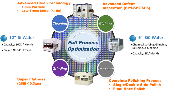
Scientech initiates its operations by meticulously categorizing different segments, with each segment subject to specific and tailored reclaim processing methodologies. Scientech's expertise in handling both silicon (Si) and silicon carbide (SiC) wafers, irrespective of whether they possess pattern or non-pattern attributes and regardless of whether they are metal (copper and silver) or non-metal deposited wafers.
Furthermore, copper-deposited wafers are exclusively processed due to their distinctive chemical properties and a deliberate strategy to ease the potential risks associated with contamination.
Each wafer undergoes multiple rounds of wet chemical stripping to eliminate patterns, surface-deposited materials, and any external defects. Following the tuned polishing step, a controlled amount of silicon is selectively removed, and polished leaving the wafer with the desired characteristics, both front and back sides are polished (if required). Upon the completion of the polishing phase, each wafer undergoes a comprehensive final cleaning using RCA cleaning techniques and effective drying ensuring its impeccable cleanliness and suitability for further processes.
Furthermore, a rigorous inspection is conducted on all wafers to identify any physical damages and assess particle sizes, upholding the highest standards of quality control according to requirements. Ultimately, management of particle size within the wafer reclaim process stands as a pivotal element in ensuring top-tier quality. Scientech's wafer reclaim process, in particular, consistently achieves a targeted particle size range of 26-19 nm (optimized for the 5 nm technology node), while simultaneously maintaining metal trace levels below 1E9. Additionally, it attains a remarkable reduction in surface roughness, GBIR of less than 0.5μm. This outstanding performance is further complemented by the capacity to process over 160,000 wafers per month, exemplifying Scientech's dedication to quality and increased production capacity contributing to the elevation of semiconductor quality.
If you have any further questions, please feel free to contact us by using Line or Email.
E-mail: info@scientech.com.tw
All the best!


