


 繁體中文
繁體中文 English
Infrared Inspection for Silicon Chipping and Cracking After Dicing or Singulation
Infrared Inspection for Silicon Chipping and Cracking After Dicing or Singulation
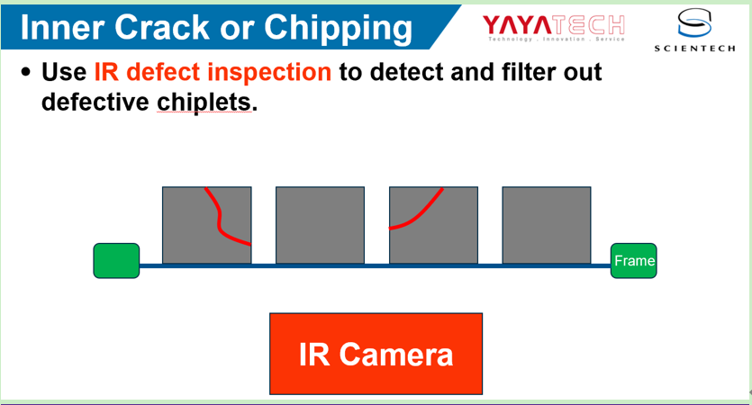
In semiconductor manufacturing, dicing or singulation is a critical process that separates individual dies from a processed wafer. Whether performed mechanically or with lasers, this step introduces significant physical stress on the wafer, which may lead to chipping or cracking of the silicon (Si) substrate. Such damage, particularly when it occurs beneath the surface, can adversely affect device performance and long-term reliability. Early and non-destructive detection of these defects is made possible by infrared (IR) inspection, now an indispensable tool in AOI.
Why Si Chipping and Cracking Matter
Post-dicing damage can manifest in several forms:
- Edge chipping: Small pieces of silicon that break away near die edges.
- Subsurface cracks: Hidden beneath the surface and invisible to the naked eye, these cracks may propagate during packaging or field operation.
- Corner breaks or full die fractures: More severe forms of damage that typically result in immediately scrapping.
These defects can lead to:
- Electrical failures caused by circuit discontinuities.
- Mechanical failures during subsequent handling or bonding processes.
- Reduced yield and increased customer returns in high-reliability applications.
Thus, early and accurate inspection is crucial.
Why Use Infrared (IR) Inspection?
Silicon is semi-transparent to infrared wavelengths (typically in the1060–6000 nm range), which makes IR inspection uniquely effective for penetrating the Si substrate and reveals subsurface features. In contrast to optical microscopy, which is limited to surface features, IR imaging can reveal buried cracks, voids, and delaminations.
Key advantages include:
- Non-destructive testing (NDT)
- High throughput for inline inspection
- Compatible with both fully processed wafers and singulated dies
IR Inspection Process Overview
- Illumination: An IR light source is directed toward the wafer or die.
- Transmission or reflection: Depending on the optical setup, the IR light is either transmitted through or reflected off the Si structure.
- Detection: An IR-sensitive camera captures the image.
- Analysis: Image processing software identifies anomalies such as cracks, voids, and inclusions.
Imaging Modes
- IR Transmission Mode: Ideal for thinned wafers or dies mounted on transparent tapes, where IR light can pass through the material.
- IR Reflection Mode: Used for thicker wafers or those on opaque carriers, as this mode captures IR light reflected off the surface or internal structures.
Integration in Manufacturing
In modern fabs, IR inspection is typically integrated inline, either immediately following dicing or prior to die attach. Some advanced packaging lines also incorporate AI-assisted IR defect classification, enabling automated die binning based on defect severity.
Typical Applications
- Si wafers used in logic, memory, CIS, and power devices
- Compound semiconductors like SiC or GaN
- 3D stacked dies and wafers with TSVs
- High-reliability ICs for automotive and aerospace
Challenges and Considerations
While IR inspection is a powerful technique, several key factors must be managed:
- Resolution limitations: Detection of microcracks <1 µm may require advanced optics.
- Throughput trade-offs: Achieving higher resolution often results in slower scan speeds.
- Tape transparency: Carrier tapes must be IR-compatible for transmission mode imaging.
Emerging technologies, such as deep learning-based defect recognition and hybrid IR/visible imaging systems, are progressively helping to overcome these limitations.
Conclusion
As semiconductor devices become thinner, more densely packed, and increasingly performance-critical, ensuring die integrity post-dicing is more important than ever. Infrared inspection offers a reliable, non-invasive, and high-throughput solution for detecting Si chipping and cracking, thereby preventing latent failures and improving final yield.
By incorporating IR inspection into the post-dicing workflow, fabs can proactively ensure the mechanical integrity of dies, reduce field returns, and maintain the high quality standards required in today’s semiconductor production
如有任何問題 歡迎來信
或是上Line官網隨時聯繫聯絡我們:info@scientech.com.tw
謝謝! 祝您順利!


