Search

Your search for "advanced energy" gave back 16 results.

Circuit board/ Robot/ Power repair and overhaul

Circuit board

Most circuit boards in semi-conductor equipment can be repaired without circuitry. Under carefully repaired, co-work with users to test it on their own equipment, there are about 80% successful rate.Truly, repaired is not difficult, its how to prevent same root cause happen again. 

In Scientech, weve experienced engineers, systematization team work and continuing improved study in order to give our customer reliable service.
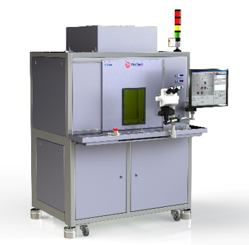
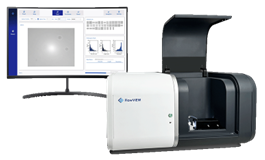
Scientech provides all kinds of suitable instrument tools without side effect such as PCB trouble shooter, In circuit Tester, BGA rework tool, capacitance tester, Power supply tester, High frequency constant temperature soldering iron, electric tin sucker, soldering pot, and microscope system, etc...

Under our professional repairing and service, your goods will optimize as a new one. Scientech appreciates to co-work with customers in any projects.For example: To modify and improve PCB abilities to reduce fail rate,and even to repair PCB which already out of production.

Key components repairing

Scientech supplies all kinds of the key components repairing. Even with the equipments we are not distributing, we also can collaboration and develop with customer.

Robot repairing

  • Scientech represents Kensington. For Kensington robot sale and repair, please refer to : Kensington automation 
  • Scientech represents Nidec-Genmark. For Nidec-Genmark robot sale and repair, please refer to : Nidec-Genmark automation

Power repair and overhaul

  • Scientech represents Dynatronix. For Dynatronix power sale and repair, please refer to : Dynatronix power
  • Scientech represents Advanced Energy (AE). For AE power sale and repair, please refer to : Advanced Energy (AE)
Content changed at :2019-08-08 11:16:17

PacTech

PacTech is a technology-focused company specialized in advanced packaging equipment manufacturing and wafer level packaging services. Since PacTech establishment, their team has been working relentlessly on developing new leading-edge technologies for the next generation applications. PacTech is known to be highly adaptive to customization and unique applications. Their team of technical experts is striving to resolve various packaging challenges faced by the industry to provide our customers and partners more competitive solutions in terms of cost, time-to-market, and technology advancement. PacTech headquarter is located in Nauen, Germany with two operation and manufacturing sites in Santa Clara, CA, USA and Penang, Malaysia. 

SB2 series–Laser Solder Jetting Equipment

SB2,植球/補球,雷射焊接,精密焊接,打線焊接

SB2 series – laser solder jetting technology is clean, precise, and flexible. The singulation disc will dispense a single solder ball into the capillary where the laser beam’s thermal energy
melts the solder ball, enabling it to fall onto any solder position and being reflowed immediately. It works with various solder alloys of different melting point and requires no flux  therefore it is clean. The localized heat and short pulse generated by the laser assures that minimal thermal stress is applied on the area beyond the joined surfaces. The single solder ball dispensing mechanism requires no tooling, hence enables flexible soldering location and contactless soldering.

Main features
  • Fluxless
  • Mask/Stencil-less
  • Clean
  • High placement accuracy
  • Contactless soldering
  • In-situ reflow for low thermal stress
Standard Certification


Application
  • BGA/PCB/cLCC Balling
  • Rework/Repair of BGA like Packages
  • MEMS & Advanced Package (2D/3D/3.5D packaging)
  • Wafer Level Packaging (Wafer Bumping/ Wafer Level CSP Bumping) 
  • TSV-Via Solder Filling/ Solder Stacking/ Sealing Processes
  • Optoelectronics/ Micro Optics/ Filter Devices/ Camera Modules/ Hard Disk Drive
Specification


LaPlace – Laser Soldering and Assembly Equipment

LaPlace,雷射焊接,黏晶,精密焊接

Using localized laser heating mechanism, temperature can be applied selectively in the interconnection areas of interest without heating up the entire substrate up to the reflow temperature to liquefy and reflow an interconnection of a few microns. With customized bond tool and laser technology, pick-and-place and assembly reflow heating are accomplished in single step at high accuracy <5µm. Localized heat ensures reliable bonding of large dies while the in-situ reflow supports ultra-small die assembly as small as 300µm.
LaPlace unique temperature control mechanism protects single chip or component from being over-heated and prevents substrate from warpage and repeating reflow circumstances.

Main features
  • Localized and selective heating with laser
  • Flexible laser beam shaping
  • High placement accuracy
  • Suitable for bonding materials with CTE-mismatch
  • Customizable bond tools
  • In-situ reflow for low thermal stress
Standard Certification


Application
  • Advanced Package (2D/3D/3.5D packaging)
  • Surface Mount Technology (SMT)
  • High presision for Filp-Chip /electronic components placement assembly
  • Probe cards assembly 
Specification


Content changed at :2023-08-28 17:12:19

Axus Technology Signs Scientech as Exclusive Distribution Partner for China and Taiwan, Expanding Global Footprint

Axus Technology Signs Scientech as Exclusive Distribution Partner for China and Taiwan, Expanding Global Footprint

Strategic Partnership Expedites Sales, Service and Support of Axus’s
CMP Processing and Cleaning Systems for Customers in Region

CHANDLER, Ariz., October 31, 2024 – Axus Technology, a leading global provider of chemical mechanical planarization (CMP) equipment, critical for semiconductor and compound semiconductor fabrication, today announced it has entered into a strategic distribution agreement with Scientech Corporation (Taipei, Taiwan). Scientech will now provide sales, installation, service, parts, process development assistance and technical support throughout China and Taiwan for Axus's Capstone CMP platform and Aquarius wafer-cleaning tools – designed specifically for processing complex compound semiconductor materials such as silicon carbide (SiC) and gallium nitride (GaN), as well as for other fast-growing markets such as advanced packaging.

In response to growing demand from key markets such as artificial intelligence (AI), renewable energy and automotive, compound semiconductor wafer production in the region is growing rapidly. According to Yole Group, China captured more than one-third of the SiC wafer and epi wafer market in 2023. Taiwan is also gaining notice for its government-funded program focused on gallium nitride epitaxial crystal growth on 200mm QST substrates (GaN-on-QST). These efforts heighten the need for capital equipment like Axus’s Capstone systems, which are optimized to meet these materials’ challenging process requirements.

“It’s exciting to see new development projects and applications in China and Asia that are  creating new opportunities for compound semiconductors,” said Axus Technology CEO Dan Trojan. “Partnering with Scientech, which represents many well-known providers of capital equipment in the region, will ensure that customers have access not only to our product offerings but also to state-of-the-art service and support.”

“Axus Technology has demonstrated impressive success in building its customer base in North America and Europe,” said MT Hsu, CEO, Scientech Corp. “We look forward to helping the company expand its presence in Asia as demand for its high-performance, innovative CMP technology continues to accelerate.”

About Scientech Corporation
Scientech Corporation was established in 1979 and has headquarters in Taipei, Taiwan, with five additional offices across Taiwan and 10 offices in China. Scientech provides full sales, installation, service, parts, process development assistance and technical support for all representing equipment, tools and products. To learn more, visit www.scientech.com.tw 

About Axus Technology
Led by its state-of-the-art Capstone® CMP and Aquarius™ wafer-cleaning platforms, Axus Technology is a recognized industry leader in designing and building modern, flexible next-generation equipment and providing custom process-development services. Axus enables companies of all sizes, from startups to high-volume manufacturers, to test, develop, and implement leading-edge solutions—particularly for novel and emerging materials—process integration schemes, products and applications. Axus’s equipment solutions range from low cost-of-ownership entry-level tools to state-of-the-art high-volume manufacturing systems. Process testing, development, optimization, and scaling are supported by our process applications lab and foundry, which includes a full array of process equipment and supporting metrology, and is staffed by the industry’s most experienced CMP team. For more information, visit www.axustech.com 

Media Contacts:
Axus Technology                                    Kiterocket 
Emilie Marenec                                      Lisa Gillette-Martin
T: 480-331-4981                                     T: 408-205-4732
E: emarenec@axustech.com                 E: lgmartin@kiterocket.com 


LineLinkedInYouTubeFaceBook

Content changed at :2024-11-04 09:49:05

Axus Technology 與 Scientech 簽約成為中國大陸和臺灣的獨家代理合作夥伴

Axus Technology Signs Scientech as Exclusive Distribution Partner for China and Taiwan, Expanding Global Footprint

Strategic Partnership Expedites Sales, Service and Support of Axus’s
CMP Processing and Cleaning Systems for Customers in Region

CHANDLER, Ariz., October 31, 2024 – Axus Technology, a leading global provider of chemical mechanical planarization (CMP) equipment, critical for semiconductor and compound semiconductor fabrication, today announced it has entered into a strategic distribution agreement with Scientech Corporation (Taipei, Taiwan). Scientech will now provide sales, installation, service, parts, process development assistance and technical support throughout China and Taiwan for Axus's Capstone CMP platform and Aquarius wafer-cleaning tools – designed specifically for processing complex compound semiconductor materials such as silicon carbide (SiC) and gallium nitride (GaN), as well as for other fast-growing markets such as advanced packaging.

In response to growing demand from key markets such as artificial intelligence (AI), renewable energy and automotive, compound semiconductor wafer production in the region is growing rapidly. According to Yole Group, China captured more than one-third of the SiC wafer and epi wafer market in 2023. Taiwan is also gaining notice for its government-funded program focused on gallium nitride epitaxial crystal growth on 200mm QST substrates (GaN-on-QST). These efforts heighten the need for capital equipment like Axus’s Capstone systems, which are optimized to meet these materials’ challenging process requirements.

“It’s exciting to see new development projects and applications in China and Asia that are  creating new opportunities for compound semiconductors,” said Axus Technology CEO Dan Trojan. “Partnering with Scientech, which represents many well-known providers of capital equipment in the region, will ensure that customers have access not only to our product offerings but also to state-of-the-art service and support.”

“Axus Technology has demonstrated impressive success in building its customer base in North America and Europe,” said MT Hsu, CEO, Scientech Corp. “We look forward to helping the company expand its presence in Asia as demand for its high-performance, innovative CMP technology continues to accelerate.”

About Scientech Corporation
Scientech Corporation was established in 1979 and has headquarters in Taipei, Taiwan, with five additional offices across Taiwan and 10 offices in China. Scientech provides full sales, installation, service, parts, process development assistance and technical support for all representing equipment, tools and products. To learn more, visit www.scientech.com.tw 

About Axus Technology
Led by its state-of-the-art Capstone® CMP and Aquarius™ wafer-cleaning platforms, Axus Technology is a recognized industry leader in designing and building modern, flexible next-generation equipment and providing custom process-development services. Axus enables companies of all sizes, from startups to high-volume manufacturers, to test, develop, and implement leading-edge solutions—particularly for novel and emerging materials—process integration schemes, products and applications. Axus’s equipment solutions range from low cost-of-ownership entry-level tools to state-of-the-art high-volume manufacturing systems. Process testing, development, optimization, and scaling are supported by our process applications lab and foundry, which includes a full array of process equipment and supporting metrology, and is staffed by the industry’s most experienced CMP team. For more information, visit www.axustech.com 

Media Contacts:
Axus Technology                                    Kiterocket 
Emilie Marenec                                      Lisa Gillette-Martin
T: 480-331-4981                                     T: 408-205-4732
E: emarenec@axustech.com                 E: lgmartin@kiterocket.com 


LineLinkedInYouTubeFaceBook

Content changed at :2024-11-04 16:55:24

FlowVIEW

FlowVIEW specializes in AI-powered particle imaging systems, integrating optics, fluidics, and AI classification.
Its solutions support high-resolution detection from micron to nanoscale, serving semiconductor, biomedical, and materials industries.
The company offers real-time analysis, customizable reports, and AI modules, enabling clients to enhance cleanliness monitoring and automation

AI Particle Imager S100

The system provides comprehensive data including particle count, size, length, roundness, and high-resolution images. It further supports AI-based classification algorithms for deep learning, enabling precise identification and categorization of various particle types.
It is ideal for applications such as process contamination monitoring and cleanliness inspection. The system supports a wide range of sample types and delivers real-time classification with statistical reporting.


Main features

Real-time monitoring of nano-scale particle distribution

Visualization of particle morphology and shape

High-speed, high-volume, and high-precision particle analysis in fluids

Five key analytical metrics for comprehensive data insight

Enhanced AI recognition for classifying hard-to-detect particles with detailed shape and morphology visualization


Application

# Trace contamination detection in semiconductor processes
# Materials: roundness, dispersion, and agglomeration analysis
# Display panels: bubble detection and fine contamination analysis
# Water quality: microorganism identification and AI-based classification
# Biomedical: cleanliness analysis of medical instruments
# Food industry: bacterial imaging and classification
# Contamination analysis in liquid and gas samples


Specification

# Measurement Range: 0.1 μm to 10 μm
# Measurement Mode: Offline / Online
# Measured Parameters: Particle size, roundness, length, particle size distribution (PSD) chart, and particle images
# System Dimensions: W795 × L512 × H643 mm (±5 m m)
# Weight: 55 kg (±5 kg) 


LEADquid Series | Imager 9000/5000/800


LEADquid Series | Imager integrating both particle sizing (Sizer) and counting (Counter) functionalities.
With advanced AI-powered defect detection, it accurately distinguishes contamination sources such as bubbles, crystals, and dust—providing visual verification and significantly reducing manual misjudgment.

The high-end AI particle imaging system is designed for automatic classification of foreign substances and particles.
It supports continuous sampling and batch analysis, making it suitable for both production line automation and laboratory sample comparison.

Main features

# Captures up to 100,000 particles per minute
# Instantly visualizes particle count, concentration, and overall size distribution in liquid samples
# Equipped with proprietary Extended Depth of Field (EDOF) optics and a high-speed microfluidic detection module for rapid particle data acquisition
# Supports multi-class AI training models
# Software is expandable with customizable algorithm modules

Standard Certification


Application

# Trace contamination detection in semiconductor processes
# Materials: roundness, dispersion, and agglomeration analysis
# Display panels: bubble detection and fine contamination analysis
# Water quality: microorganism identification and AI-based classification
# Biomedical: cleanliness analysis of medical instruments
# Food industry: bacterial imaging and classification
# Contamination analysis in liquid and gas samples

Specification

# Measurement Range: 0.8 μm to 400 μm
# Measurement Mode: Offline / Online
# Measured Parameters: Particle Count, size, roundness, length, Aspect Ratio, and particle images
# System Dimensions: 476 x 364 x 298 mm (±5mm)
# Weight: 23 kg (±5 kg)


Multi-channel Liquid Particle Counter (MLPC) 


An online wet-process micro-particle automation monitoring solution that provides continuous, long-term particle count monitoring and real-time trend insights across process stages. 

Main features

# Online 24-hour monitoring of particle counts to capture trends across process stages. 

# Establish stable process standards: basis for tool maintenance and process stability; built-in auto data storage for one year. 

# One device, multi-point monitoring with 9 detection channels; integrable with existing production tools to lower equipment cost. 

# Defect prediction / Auto alarm: threshold-triggered alerts with real-time data feedback; supports preventive maintenance (e.g., filter change) to reduce abnormal-loss cost. 

# Compatible liquids: developer, mixed-acid PR remover, copper/aluminum acids, DI water, etc. 

 
Application

# Quality control stages: incoming (IQC); in-process and outbound (IPQC, PQC, OQC). 
# Chemicals/Media: IPA, stripping agents, developer, KOH cleaner, remover (stripper), electroless/electroplating solutions, DI water, metal etchant, stripper, copper acid, aluminum acid. 
# Wafer manufacturing: etching, stripping, lithography, cleaning.
# PCB: electroless/electroplating, etching, stripping.
Packaging: cleaning. 


Specification

Particle size range 0.1 μm – 100 μm
Detection channels 9
Cleaning channel 1
Sample temp/viscosity 5–80 °C / 150 cps
Particle concentration limit 4,000 P/ml @ 5% coincidence error
Dimensions W850 × L550 × H1629 mm (±5 mm)
Weight 105 kg (±5 kg)
Options De-bubbles / Liquid recirculation system


Uses exclusive nano-membrane to create an atmospheric chamber inside the SEM vacuum, preserving the original state of liquid samples without drying. With analysis software, it outputs particle size distribution, dispersion/aggregation, shape, and EDS-assisted composition; highest liquid-phase resolution detects 7 nm particles, streamlining workflows and shortening development time.

Main features

# Preserve liquids under SEM with the nano-membrane atmospheric chamber.
# Integrated analysis with FlowVIEW Lite: size distribution, dispersion/aggregation, concentration, shape, composition (with EDS).
# Resolution: liquid-phase detection down to 7 nm.
# Compatibility: 99% with major SEM brands/models (FEI, ThermoFisher, Keyence, JEOL, Hitachi, ZEISS, Phenom, TESCAN…) and relevant preparation tools.
# Ease of use: sample sealing in 30 seconds.

Standard Certification


Application

# Industries: Semiconductor, Energy, Biopharma. 
# Example materials: Metal plating, CMP slurry, coating materials, solder paste, silver paste, aluminum, copper paste, MLCC, probiotics, pheromone, black mold, fungus spores.


Content changed at :2025-08-20 15:50:16

TME

TM Electronics has been in the business of manufacturing measuring instruments for over 60 years. We’ve spent that time inventing brilliant devices that can improve both the quality and productivity of your processes. 
We started out in the metal fabrication industry where we specialized for 20 years. In the early eighties we saw an opportunity to create medical devices and expand our measuring device portfolio. Thankfully, we grasped it and the move broadened our horizons. Soon the innovative minds of our engineers were imagining new devices to improve the automotive, electronics, pharmaceutical, and food manufacturing markets. 
Now we manufacture the best in automated, high technology leak testers, leak and flow testers, and package testers.

TME Integra Flex

TME’s Integra Flex instruments offer you an affordable method of leak testing that is perfect for different testing environments. You can configure the industrial rack-mount model for easy integration into OEM operations, data , and connectivity tools. The benchtop model is perfect for smaller production environments and R&D applications.

Main features
  • Easy LAN connectivity
  • Rack mountable
  • Standard XML data format
  • Compact size
  • Remote control options for factory integration
  • PLC controls and I/O for user operations
  • Easy integration into Quality Control tools and I.O.T systems
Standard Certification


Application
  • Applications: Leak Testing
  • Industries: Beverage, Flexible Packaging, Food
Specification

Integra Flex 01 Pressure Range:  0-100 psig
Integra Flex 01 accuracy:  ± 0.5 psi
Integra Flex 02 Pressure Range:  -14.7 to +15 psig
Integra Flex 02 accuracy:  ± 0.15 psi
Integra Flex 03 Pressure Range:  ATM to -14.7 psi vacuum
Integra Flex 03 accuracy:  ± 0.1 psi
Resolution: 0.0001 psi
Mains Power:  Desktop 12 vdc Industrial 24 vdc
Test port fitting:  1/8” FNPT
Interface Communications/Connectivity:  Ethernet TCP/IP, RS232, I/O (8I/O)
HMI:  8” Touchscreen accessory
Regulator:  Manual Regulator

LT-V/L_TME WORKER Integra

The smart TME WORKER Integra is an intelligent instrument making programming, testing, downloading, printing, storing, accessing, reviewing test results much easier than it has been done in the past.

Main features
  • High resolution (0.0001 psi)
  • The small internal volume contributes to high sensitivity, repeatability, and reliability.
  • The Icon-Based Touchscreen Color Display allows the operator to control the test parameters, examine statistical analysis of results or download data files easily.
  • USB Connection to a PC
  • USB ports for keyboard, Mouse, Printer or bar code reader
  • LAN remote instrument control, data transfer, and operation
  • Optional electronic regulator available
  • The smart TME WORKER Integra is an intelligent instrument making programming, testing, downloading, printing, storing, accessing, reviewing test results much easier than it has been done in the past.
Standard Certification

ASTM D4991
ASTM D5094
ASTM F2095
ASTM F2096
F-1140
F-2054
FDA CFR 21 part 11
IEC 60529 (IP67 Equivalency testing)
ISO 11607

Application
  • Applications:Creep to Fail Testing, Integrity Testing, Leak Testing
  • Industries:Aerospace, Automotive, Defense, Electronics, Flexible Packaging, Food, Industrial, Medical Devices, Pharmaceutical
Specification

Small Footprint: 10"Wx10"Dx9"H
Security Controls: Key Lock
Display: 5.7” QVGA Color Touchscreen
Pressure Control: Manual or Electronic
Units: Psig, InH2O, mBar, kPa, inHg, ccm, LPM, cfm
Test Modes: Leak, Flow, Occlusion
Memory Capacity: 128 Mbytes (Expandable up to 512Mb)
LAN (Network):  Web-browser & more
Test Modes: Leak, Occlusion, Flow
Range (PSIG):  -13.5 to 150
Resolution (PSIG):  0.0001 (-13,5 to 150)
Pressure Accuracy:  +/- 0.5% FSD
Repeatability (6 sigma/FSD):  <1%
Flow Ranges (SCCM): up to 10.000
Flow Accuracy: +/- 2% FSD

PA-2096 TME Pressure Bubble Tester

The TM Electronics TME Pressure Bubble Tester provides low pressure and controlled flow to a pouch to meet the requirements of ASTM International F-2096 test method “Standard Test Method for Detecting Gross Leaks in Packaging by Internal Pressurization Bubble Test”.

Main features
  • Meets ASTM F-2096 Standards
  • Simple set up
  • Open screen retainer provides high visibility from all sides
  • Retainer is locked in position to hold the pouch underwater
  • Digital pressure readings – multiple units of measure with backlighted display
  • Low pressure control 2" H2O
  • NIST traceable gauge calibration
Standard Certification

ASTM D5094
ASTM F2096

Application
  • Applications: Creep to Fail Testing, Integrity Testing, Leak Testing
  • Industries: Aerospace, Automotive, Defense, Electronics, Flexible Packaging, Food, Industrial, Medical Devices,  Pharmaceutical
Specification

Control box:  Low Pressure Regulator
Bubble Testing: ASTM F2096
Pressure levels: 0.1 to 5 PSIG

BT-IP BT Integra Pack: Smart Package Tester

TME Smart BT Integra-Pack-Package Tester for Burst Tests, Creep Tests, Creep-to-Failure Tests, and Leak Integrity Tests

Main features
  • A bench-top, high-resolution (0.001 psig) test instrument
  • A small footprint and user-friendly ease of operation
  • Electronic pressure and flow controls provide precise and repeatable test conditions
  • Automatic and high flow output allow testing of large porous packages
  • Applications cover a range of flexible or rigid, porous and non-porous, open or sealed packages.
  • Complies with standards for all commonly-used Seal Strength and Package Integrity tests (Burst, Creep, Creep-to-Failure, and Leak Integrity)
  • Automatic Burst Test Mode
  • Results right out of the box, no lengthy setup
  • Senses package size during prefill
  • Manual Burst Test Mode
  • Multiple levels of control for optimal test results – Ramp Rate, Porous vs. Non-Porous Packages, Max/Min Acceptance Limits, Pressure Drop Sensitivity
  • High Performance
  • Advanced, user-defined smart interface compatible with USB keyboards, mice, bar code readers
  • Low Power Stand-by Mode for energy conservation
  • Graphical test plot display for leak, burst and creep tests
  • Test data exporting to PC using Flash Driv
Standard Certification

ASTM F2095
ASTM F2096
F-1140
F-2054
FDA CFR 21 part 11
ISO 11607

Application
  • Applications:Burst Testing, Creep to Fail Testing, Leak Testing, Strength Testing
  • Industries:Flexible Packaging, Food, Medical Devices, Pharmaceutical
Specification

Resolution:  Higher Pressure Resolution (0.01 psi burst, 0.001 leak)
Regulator:  Automatic Regulator (fast pressure setting)
Flow capacity:  High Flow Capacity (up to 15 CFM)
Pressure:  Low Pressure Sensitivity at 5 InH2O
Display:  High Resolution Color LCD Display with Touchscreen
Metric units:  Standard and Metric units

Content changed at :2024-01-11 10:38:00

Pages