


 繁體中文
繁體中文 English
辛耘知識分享家:VLSI標準片介紹及校正服務新知
辛耘知識分享家
VLSI標準片介紹及校正服務新知
2023年03月電子報
VLSI標準片介紹
在半導體、化合物半導體、面板和LED製造領域中,各種量測設備的使用至關重要,以確保產品的品質和性能。為了維持量測結果的準確性和可靠性,一套標準片對於校準和驗證量測儀器而言,無疑是必要的。
這些標準片對於設備的維護與校正具有重要意義。它們具有一定的規格和尺寸,經過精密測量和標準化的過程,用於與測量儀器進行對照和校正。
校正服務是量測工程中的另一個關鍵方面。良好的校正服務可以確保量測設備不僅在生產過程中始終維持高精度,而且有助於保持產品的整體品質。專業的校正服務提供商會定期評估量測設備的性能,並提供所需的維修和校準,以確保設備始終運行在最佳狀態。
產品分類
階高標準片(Step Height Standards)
膜厚標準片(Film Thickness Standards)
線寬標準片(Nano CD Standards)
微粒標準片(Absolute Contamination Standards)
阻值標準片(Resistivity Standards)
應力標準片(Stress Standards)

校正服務:
校正服務是量測工程中的另一個關鍵方面。良好的校正服務可以確保量測設備不僅在生產過程中始終維持高精度,而且有助於保持產品的整體品質。專業的校正服務提供商會定期評估量測設備的性能,並提供所需的維修和校準,以確保設備始終運行在最佳狀態。
半導體、化合物半導體、面板和LED領域中產品的高品質和性能,取決於嚴格的量測標準和專業的校正服務。設備的校準和維護,有助於輸出穩定且可靠的產品,並確保生產線的高效運行。因此,在這個競爭激烈的市場中,廠商應依賴標準片和校正服務,以確保全面提升產品品質。
VLSI公司簡介
VLSI公司成立年份:1984年
地點:美國加州之MILPITAS
總銷售: 超過500萬片之標準片
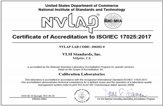
第三方認證單位:美國NIST國家級實驗室

Contamination Products:
|
||
|
||
|
||
|
||
|
||
|
||
|
||
|


Film Thickness Products:
|
||
|
Dimensional Products:
|
||
|
||
|
||
|
||
|
||
|
||
|
||
|
||
|
||
|
||
|
Electrical Products:
|
||
|
Solar Products:
|
|
Solar / Photovoltaic Products |
Technical Papers:
- Accurate and Reliable Optical CD of MuGFET down to 10 nm
IMEC,VLSI Standards, Proc. Of SPIE Vol. 6518*
- Comprehensive Approach to MuGFET Metrology
IMEC, KLA-Tencor, VLSI Standards, Proc. Of SPIE Vol. 6152*
- CD Measurement of Angled Lines on High-End Masks and its Calibration Method
Holon Co., Ltd., Proc. Of SPIE Vol. 5992*
- Sub-50 nm Isolated Line and Trench Width Artifacts for CD Metrology
KLA-Tencor, VLSI Standards, Proc. Of SPIE Vol. 5375*
- NIST-Traceable Calibration of CD-SEM Using a 100 nm Pitch Standard
VLSI Standards, Proc. Of SPIE Vol. 5038*
- Metrology Standards for Semiconductor Manufacturing
VLSI Standards, IEEE 0-7803-8511/X/04**
- 100 nm Pitch Standard Characterization for Metrology Applications
VLSI Standards, Proc. Of SPIE Vol. 4689*
- Characterization of an 100 nm 1D Pitch Standard by Metrological SEM and SFM
Physikalisch-Technische Bundesanstalt (PTB), VLSI Standards, Proc. Of SPIE Vol. 5375*
- Reticle Programmed Defect Size Measurement using Low-Voltage SEM and pattern recognition techniques
KLA Tencor, VLSI Standards, Proc. Of SPIE Vol. 3996*
- Development of the Nitride Film Thickness Standard (NFTS)
VLSI Standards, Proc. Of SPIE Vol. 3479*
- Development of a Physical Haze and Microroughness Standard
VLSI Standards, Proc. Of SPIE Vol. 2862*
- Measurement of a CD and Sidewall Angle Artifact with Two-Dimensional CD-AFM Metrology
National Institute of Standards and Technology (NIST), Digital Semiconductor, Univ. of Maryland, VLSI Standards, Veeco Metrology, Proc. Of SPIE Vol. 2725*
- Polarization of out-of-plane Optical Scatter from SiO2 Films Grown on Photolithographically-Generated Microrough Silicon
National Institute of Standards and Technology (NIST), VLSI Standards, Proc. Of SPIE Vol. 3426*
- Selection of Calibration Particles for Scanning Surface Inspection Systems
Sematech, National Institute of Standards and Technology (NIST), VLSI Standards, Proc. Of SPIE Vol. 2862*
- Reticle Defect Size Calibration using Low-Voltage SEM and pattern recognition techniques for sub-200 nm Defects
KLA Tencor, VLSI Standards, Proc. Of SPIE Vol. 3873*
- Numerical Simulation of Thick Line Width Measurements by Reflected Light
Weidlinger Associates, Sematech, VLSI Standards, Proc. Of SPIE Vol. 1464*
- Model of Light scattering Structures with Particle Contaminants
Arizona State University, Proc. Of SPIE Vol. 2862*
- Development of a Smooth-Surface Microroughness Standard
ADE Optical, VLSI Standards, Proc. Of SPIE Vol. 3141*
- Reticle Defect Sizing of Optical Proximity Correction Defects Using SEM Imaging and Image Analysis Techniques
KLA Tencor, VLSI Standards, Proc. Of SPIE Vol. 4066*
- A New Line Width Standard for Refelected Light Inspection
CD Metrology, Inc., VLSI Standards, Proc. Of SPIE Vol. 1464*