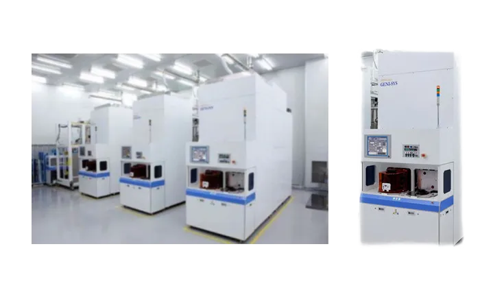
HPSP (High Pressure Solution Provider) is a leading Korean equipment manufacturer specializing in high-pressure annealing technologies for the global semiconductor industry. Its flagship product is a vertical furnace engineered for advanced high-pressure anneal processes.
HPSP pioneered the world's first and only H2/D2 high-pressure anneal technology. This breakthrough addresses critical challenges in advanced node manufacturing for both logic and memory applications.
Beyond its core annealing technology, HPSP operates a robust global sales and service network across the United States, Europe, and Asia, offering comprehensive customer support throughout the semiconductor value chain.

The GENI-Sys System is a vertically oriented, high-pressure, fully automated thermal processing furnace designed for 200 mm and 300 mm wafer applications. Engineered to meet the semiconductor industry's latest standards for equipment design, cleanliness, manufacturing, and process control, the GENI-Sys ensures reliable performance in demanding manufacturing environments.
Capable of processing at up to 25 ATM, this system delivers exceptional annealing effects at temperatures below 450°C, making it ideal for applications where thermal budget constraints are critical.
- Supports 200 mm or 300 mm wafers with cassette loading configuration
- Dry gas operation is standard; optional steam environment available
- Flexible wafer handling for front-side or back-side processing
- External boiler available for wet process requirements


