Semiconductor companies encounter substantial expenses in constructing facilities and acquiring equipment, resulting in a capital-intensive industry. To remain competitive and keep up with the most recent technological advancements, semiconductor companies must continually discover innovative ways to optimize their spending and reduce capital expenses without jeopardizing the quality, and effectiveness of their technology and equipment investments.
In order to minimize capital spending within the semiconductor sector, it is vital to efficiently optimize equipment utility. One way to achieve this objective is to create equipment designed specifically for the necessary tasks, thereby avoiding unnecessary expenses. Furthermore, process optimization plays a crucial role in identifying opportunities to enhance efficiency, including decreasing cycle times, increasing yields and minimizing waste. By implementing these actions, semiconductor companies can reduce capital spending while still accomplishing their desired objectives.
In the semiconductor sector, outsourcing non-essential tasks, such as designing and manufacturing the process equipment, to dedicated third-party companies can aid in reducing the substantial costs associated with the equipment and facilities required for such operations. Outsourcing also offers access to specialist knowledge and skills that may not be accessible in-house, resulting in better product and service quality. Working in conjunction with other firms also presents opportunities to gain access to new technologies and expertise that may not be readily available, particularly for emerging firms and startups.
Through the implementation of process improvements, semiconductor firms can successfully decrease their capital expenditure. One method of achieving this is through a constant refinement of their manufacturing processes to improve efficiency and reduce waste. To accomplish this, companies may adopt methodologies such as Six Sigma, which focuses on decreasing defects and enhancing quality.
The semiconductor industry is facing increasing pressure with high capital expenditure while maintaining competitiveness. The approaches discussed above, including equipment optimization, outsourcing, collaboration, partnership, lean manufacturing, and process improvements, can all help to minimize expenditure while still investing in the latest technology and equipment. By adopting these approaches, semiconductor companies can improve efficiency, reduce waste, and free up capital for other purposes, ultimately leading to increased competitiveness and profitability.
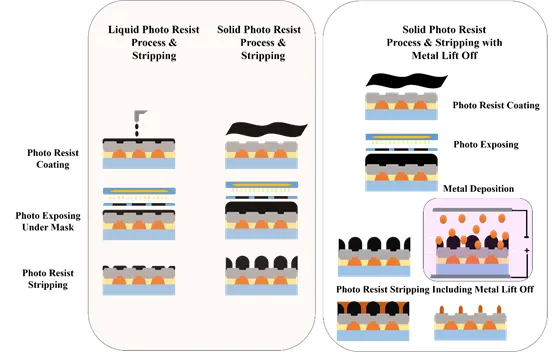
In modern semiconductor process, removing the photoresist is a critical step. After the lithography process, the exposed photoresist must be removed from the wafer surface to reveal the patterned areas for further processing.
With modern semiconductor technology, the size of the active area continues to decrease, resulting in more complexity during the lithography process. The patterned features become smaller and more densely packed, making the removal of photoresist a more challenging task as it needs to be done with care to prevent any damage to the underlying substrate or patterned features.
Scientech is a semiconductor equipment merchandiser with over 40 years of experience. We specialize in developing and manufacturing precision packaging equipment and wafer bonding solutions for over 15 years. Our latest product, the PR Stripper (soak and spray module), has been hybridized and updated to produce a high-quality output as a single wafer process while maintaining a high yield quantity as a bench process. Our hybridized PR stripper offers the capability to monitor and regulate the process of a specific individual wafer or a required set of wafers. Moreover, it enables the simultaneous use of wafers of different sizes, such as 8-inch and 12-inch wafers. Through extensive research and data surveying, we have developed a PR stripper that effectively removes solid and liquid film resist products in a cost-effective and efficient manner, as represented in Figure.
The chemical solution dissolves residues and photoresists, while insoluble metals are lifted off. When using conventional PR resist tools, managing the chemicals and the residues floating on the chemical tank can significantly impact the yield. However, with Scientech's hybridized PR stripper, we have designed immersion tanks that can effectively handle residues. We have also incorporated dual long-lasting filters to reduce chemical wastage while maintaining the filtration process's efficiency. Additionally, multiple robotic arms are used to handle both dry and wet wafers, thereby preventing any contamination.
Once the soaking process is complete, the wafers are parched and transferred to the spraying process. During this process, the wafers are subjected to a sequence of sprays with stripping chemicals, isopropyl alcohol-IPA, DI water, and hot nitrogen (for drying). All the spraying modules are furnished with a pressure and spraying time system that can be attuned to suit specific requirements.
Scientech's PR stripper has been deliberately designed with programmable modules that can be tailored to tune the soak and spray process, enabling it to handle various thicknesses of PR with a single tool to meet different requirements.
Our expertise lies in customizing equipment to meet the unique needs of each individual client.


