


 繁體中文
繁體中文 English
Camtek FRT

Camtek is a leading developer and manufacturer of high-end inspection and metrology equipment for the semiconductor industry.
Camtek’s systems inspect and measure wafers throughout the production process of semiconductor devices, covering the front and mid-end, and up to the beginning of assembly (Post Dicing Inspection and Metrology).
Camtek’s systems inspect wafers for the most demanding semiconductor market segments, including Advanced Interconnect Packaging, Memory, CMOS Image Sensors, MEMS, and RF, serving the industry’s leading global IDMs, OSATs, and foundries.
Camtek’s world-class sales and customer support infrastructure is organized around eight subsidiaries based in the US, Europe, Japan, China, Hong Kong, Taiwan, Korea, and Singapore.
Camtek’s inspection and metrology systems can detect defective ICs reliably at high-throughput, ensuring that only known-good-die are delivered to its customers’ final products.
With the growth in advanced packaging technologies, which have proven to be the most effective solutions for high-end products, Camtek provides various inspection and metrology technologies that can be tailored to its customers’ needs quickly and efficiently, helping them to meet the most stringent demands of defect-free products as well as supporting demand growth and time to market.
- FRT Microprof
FRT Microprof
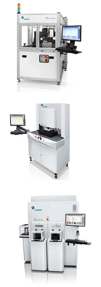
The FRT MicroProf series is a metrology solution designed for the semiconductor industry to measure wafer thickness, TTV (Total Thickness Variation), Bow, and Warp. This equipment utilizes a white light source and features an upper and lower dual-probe design. During measurement, the wafer is placed between the two probes, allowing a single test to quickly provide comprehensive geometric parameters, including thickness, TTV, Bow, Warp, TIR (Total Indicated Runout), and LTV (Local Thickness Variation).
Additionally, the system can be equipped with an infrared (IR) probe, which can penetrate materials such as Si (silicon) and GaAs (gallium arsenide), enabling thickness monitoring before and after the backside thinning process. With its high-precision measurement capability, non-contact measurement method, fast testing speed, and SEMI-compliant dual-probe design, the FRT MicroProf series has achieved a str
Main features
◆ The standard fixture is suitable for samples ranging from 2 inches to 12 inches.
◆ Capable of measuring thickness, TTV, Bow, and Warp for both opaque and transparent materials.
◆ The optional IR (infrared) probe can penetrate materials such as Si/GaAs and measure the thickness of specific layers.
◆ Applicable for: incoming inspection of Si/GaAs substrates, EPI (epitaxy) process monitoring, and backside thinning process control.
◆ Available in both manual configurations (MicroProf 200/300) and automated transfer mode (MicroProf 200/300 MHU).
◆ Equipped with a mapping function that enables multi-point measurements and generates wafer test mapping results.
◆ Built-in standard reference wafers for thickness calibration, ensuring easy, accurate, and fast calibration.
Standard Certification
Application
◆ Compound Semiconductors: GaAs, InP, SiC, GaN
◆ Front-End Silicon Devices: Power devices, MEMS, RF MEMS
◆ Back-End Silicon Devices: 8” and 12” packaging and bumping lines
◆ Optical Communication: Quartz materials